JAJSPD6K april 1998 – february 2023 SN74LV574A
PRODMIX
- 1 特長
- 2 アプリケーション
- 3 概要
- 4 Revision History
- 5 Pin Configuration and Functions
-
6 Specifications
- 6.1 Absolute Maximum Ratings
- 6.2 ESD Ratings
- 6.3 Recommended Operating Conditions
- 6.4 Thermal Information
- 6.5 Electrical Characteristics
- 6.6 Timing Requirements, VCC = 2.5 V ± 0.2 V
- 6.7 Timing Requirements, VCC = 3.3 V ± 0.3 V
- 6.8 Timing Requirements, VCC = 5 V ± 0.5 V
- 6.9 Switching Characteristics, VCC = 2.5 V ± 0.2 V
- 6.10 Switching Characteristics, VCC = 3.3 V ± 0.3 V
- 6.11 Switching Characteristics, VCC = 5 V ± 0.5 V
- 6.12 Noise Characteristics
- 6.13 Operating Characteristics
- 6.14 Typical Characteristics
- 7 Parameter Measurement Information
- 8 Detailed Description
- 9 Application and Implementation
- 10Device and Documentation Support
- 11Mechanical, Packaging, and Orderable Information
パッケージ・オプション
デバイスごとのパッケージ図は、PDF版データシートをご参照ください。
メカニカル・データ(パッケージ|ピン)
- DGV|20
- DB|20
- NS|20
- PW|20
- DW|20
- RGY|20
サーマルパッド・メカニカル・データ
- RGY|20
発注情報
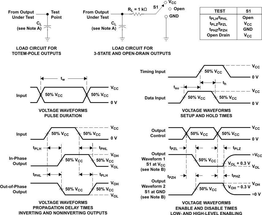
7 Parameter Measurement Information

A. CL includes probe and
jig capacitance.
B. Waveform 1 is for an output with
internal conditions such that the output is low, except when disabled by the
output control.
Waveform 2 is for an output with internal conditions such that the output is high, except when disabled by the output control.
Waveform 2 is for an output with internal conditions such that the output is high, except when disabled by the output control.
C. All input pulses are supplied by
generators having the following characteristics: PRR ≤ 1 MHz, ZO = 50
Ω, tr ≤ 3 ns,
tf ≤ 3 ns.
tf ≤ 3 ns.
D. The outputs are measured one at a
time, with one input transition per measurement.
E. tPLZ and
tPHZ are the same as tdis.
F. tPZL and
tPZH are the same as ten.
G. tPHL and
tPLH are the same as tpd.
H. All parameters and waveforms are
not applicable to all devices.
Figure 7-1 Load
Circuit and Voltage Waveforms