JAJSP17A december 2022 – april 2023 SN74LV8T245-Q1
PRODUCTION DATA
- 1 特長
- 2 アプリケーション
- 3 概要
- 4 Revision History
- 5 Pin Configuration and Functions
-
6 Specifications
- 6.1 Absolute Maximum Ratings
- 6.2 ESD Ratings
- 6.3 Recommended Operating Conditions
- 6.4 Thermal Information
- 6.5 Electrical Characteristics
- 6.6 Switching Characteristics - 1.8-V VCC
- 6.7 Switching Characteristics - 2.5-V VCC
- 6.8 Switching Characteristics - 3.3-V VCC
- 6.9 Switching Characteristics - 5-V VCC
- 6.10 Noise Characteristics
- 6.11 Typical Characteristics
- 7 Parameter Measurement Information
- 8 Detailed Description
- 9 Application and Implementation
- 10Power Supply Recommendations
- 11Layout
- 12Device and Documentation Support
- 13Mechanical, Packaging, and Orderable Information
パッケージ・オプション
デバイスごとのパッケージ図は、PDF版データシートをご参照ください。
メカニカル・データ(パッケージ|ピン)
- RKS|20
- PW|20
- DGS|20
サーマルパッド・メカニカル・データ
発注情報
7 Parameter Measurement Information
Phase relationships between waveforms were chosen arbitrarily. All input pulses are supplied by generators having the following characteristics: PRR ≤ 1 MHz, ZO = 50 Ω.
For clock inputs, fmax is measured when the input duty cycle is 50%.
The outputs are measured one at a time with one input transition per measurement.

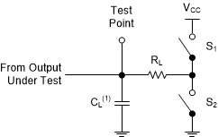
(1) CL includes probe and test-fixture capacitance.
Figure 7-1 Load Circuit for 3-State Outputs
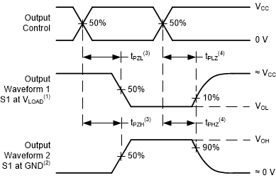
(1) S1 = CLOSED, S2 =
OPEN.
(2) S1 = OPEN, S2 =
CLOSED.
(3) The greater between
tPZL and tPZH is the same as
ten.
(4) The greater between
tPLZ and tPHZ is the same as
tdis.
Figure 7-3 Voltage Waveforms Propagation Delays
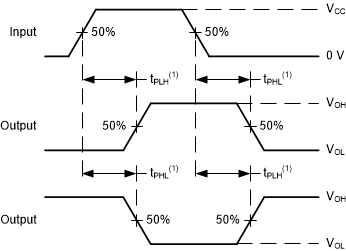
(1) The greater between tPLH and tPHL is the same as tpd.
Figure 7-2 Voltage Waveforms Propagation Delays
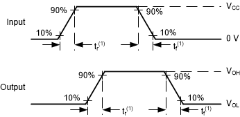
(1) The greater between tr and tf is the same as tt.
Figure 7-4 Voltage Waveforms, Input and Output Transition Times