SCES464G June 2003 – August 2015 SN74LVC1G19
PRODUCTION DATA.
- 1 Features
- 2 Applications
- 3 Description
- 4 Revision History
- 5 Pin Configuration and Functions
- 6 Specifications
- 7 Parameter Measurement Information
- 8 Detailed Description
- 9 Application and Implementation
- 10Power Supply Recommendations
- 11Layout
- 12Device and Documentation Support
- 13Mechanical, Packaging, and Orderable Information
パッケージ・オプション
デバイスごとのパッケージ図は、PDF版データシートをご参照ください。
メカニカル・データ(パッケージ|ピン)
- DBV|6
- DRL|6
- YZP|6
- DCK|6
- DRY|6
サーマルパッド・メカニカル・データ
- DRY|6
発注情報
8 Detailed Description
8.1 Overview
This decoder/demultiplexer is designed for 1.65-V to 5.5-V VCC operation.
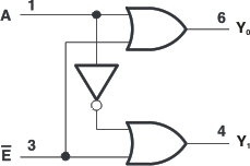
The SN74LVC1G19 device is a 1-of-2 decoder/demultiplexer. This device decodes the 1-bit address on input A and places a logic low on the matching address output, Y0 or Y1 , when the enable (E) input signal is low.
This device is fully specified for partial-power-down applications using Ioff. The Ioff circuitry disables the outputs, preventing damaging current backflow through the device when it is powered down.
NanoFree package technology is a major breakthrough in IC packaging concepts, using the die as the package.
8.2 Functional Block Diagram

8.3 Feature Description
SN74LVC1G19 is available in NanoFree package. NanoFree is a major breakthrough in IC packaging concepts, it is a bare die package developed for applications that require the smallest possible package. The device supports 5-V VCC Operation. All Inputs accept voltages up to 5.5 V. ±24-mA output drive at 3.3 V. The maximum time propagation delay (tpd ) is 5.4 ns at 3.3 V. Low Power Consumption, 10-μA Max ICC. Typical output ground bounce (VOLP ) and Output VOH Undershoot (VOHV). This device is fully specified for partial-power-down applications using Ioff. The Ioff feature ensures that damaging current will not backflow through the device when it is powered down. The SN74LVC1G19 device has isolation during power off. Ioff supports live insertion, partial-power-down mode and back drive protection.
8.4 Device Functional Modes
Table 1 lists the functional modes of the SN74LVC1G19.
Table 1. Function Table
| INPUTS | OUTPUTS | ||
|---|---|---|---|
| E | A | Y0 | Y1 |
| L | L | L | H |
| L | H | H | L |
| H | X | H | H |