SCES528F December 2003 – May 2017 SN74LVC1G373
PRODUCTION DATA.
- 1 Features
- 2 Applications
- 3 Description
- 4 Revision History
- 5 Pin Configuration and Functions
-
6 Specifications
- 6.1 Absolute Maximum Ratings
- 6.2 ESD Ratings
- 6.3 Recommended Operating Conditions
- 6.4 Thermal Information
- 6.5 Electrical Characteristics
- 6.6 Timing Requirements: TA = -40°C to +85°C
- 6.7 Timing Requirements: TA = -40°C to +125°C
- 6.8 Switching Characteristics: TA = -40°C to +85°C
- 6.9 Switching Characteristics: TA = -40°C to +85°C
- 6.10 Switching Characteristics: TA = -40°C to +125°C
- 6.11 Operating Characteristics
- 6.12 Typical Characteristics
- 7 Parameter Measurement Information
- 8 Detailed Description
- 9 Application and Implementation
- 10Power Supply Recommendations
- 11Layout
- 12Device and Documentation Support
- 13Mechanical, Packaging, and Orderable Information
パッケージ・オプション
デバイスごとのパッケージ図は、PDF版データシートをご参照ください。
メカニカル・データ(パッケージ|ピン)
- DBV|6
- YZP|6
- DCK|6
サーマルパッド・メカニカル・データ
発注情報
8 Detailed Description
8.1 Overview
A buffered output-enable (OE) input can be used to place the output in either a normal logic state (high or low logic levels) or the high-impedance state. In the high-impedance state, the output neither loads nor drives the bus lines significantly. The high-impedance state and increased drive provide the capability to drive bus lines without interface or pullup components. To ensure the high-impedance state during power up or power down, OE should be tied to VCC through a pullup resistor; the minimum value of the resistor is determined by the current-sinking capability of the driver. This device is fully specified for partial-power-down applications using Ioff. The Ioff circuitry disables the outputs, preventing damaging current backflow through the device when it is powered down.
8.2 Functional Block Diagram
 Figure 4. Logic Diagram (Positive Logic)
8.3 Feature Description
8.3.1 Balanced High-Drive CMOS Push-Pull Outputs
A balanced output allows the device to sink and source similar currents. The high drive capability of this device creates fast edges into light loads so routing and load conditions should be considered to prevent ringing. Additionally, the outputs of this device are capable of driving larger currents than the device can sustain without being damaged. It is important for the power output of the device to be limited to avoid thermal runaway and damage due to over-current. The electrical and thermal limits defined the in the Absolute Maximum Ratings must be followed at all times.
8.3.2 Standard CMOS Inputs
Standard CMOS inputs are high impedance and are typically modelled as a resistor in parallel with the input capacitance given in the Electrical Characteristics. The worst case resistance is calculated with the maximum input voltage, given in the Absolute Maximum Ratings, and the maximum input leakage current, given in the Electrical Characteristics, using ohm's law (R = V ÷ I).
Signals applied to the inputs need to have fast edge rates, as defined by Δt/Δv in Recommended Operating Conditions to avoid excessive currents and oscillations. If a slow or noisy input signal is required, a device with a Schmitt-trigger input should be utilized to condition the input signal prior to the standard CMOS input.
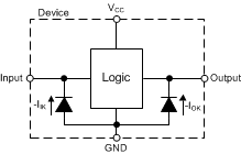
8.3.3 Clamp Diodes
The inputs and outputs to this device have negative clamping diodes.
CAUTION
Voltages beyond the values specified in the Absolute Maximum Ratings table can cause damage to the device. The input negative-voltage and output voltage ratings may be exceeded if the input and output clamp-current ratings are observed.
 Figure 5. Electrical Placement of Clamping Diodes for Each Input and Output
8.3.4 Partial Power Down (Ioff)
The inputs and outputs for this device enter a high impedance state when the supply voltage is 0 V. The maximum leakage into or out of any input or output pin on the device is specified by Ioff in the Electrical Characteristics.
8.3.5 Over-voltage Tolerant Inputs
Input signals to this device can be driven above the supply voltage so long as they remain below the maximum input voltage value specified in the Absolute Maximum Ratings.
8.4 Device Functional Modes
Table 1 lists the functions of this device.
Table 1. Function Table
| INPUTS | OUTPUT Q |
||
|---|---|---|---|
| OE | LE | D | |
| L | H | L | L |
| L | H | H | H |
| L | L | X | Q0 |
| H | X | X | Hi-Z |