SCES222Q April 1999 – June 2017 SN74LVC1G86
PRODUCTION DATA.
- 1 Features
- 2 Applications
- 3 Description
- 4 Revision History
- 5 Pin Configuration and Functions
- 6 Specifications
- 7 Parameter Measurement Information
- 8 Detailed Description
- 9 Application and Implementation
- 10Power Supply Recommendations
- 11Layout
- 12Device and Documentation Support
- 13Mechanical, Packaging, and Orderable Information
パッケージ・オプション
デバイスごとのパッケージ図は、PDF版データシートをご参照ください。
メカニカル・データ(パッケージ|ピン)
- DBV|5
- DCK|5
- DRL|5
- YZP|5
サーマルパッド・メカニカル・データ
発注情報
8 Detailed Description
8.1 Overview
The SN74LVC1G86 device performs the Boolean function Y = AB + AB in positive logic. This single 2-input exclusive-OR gate is designed for 1.65-V to 5.5-V VCC operation.
A common application is as a true and complement element. If the input is low, the other input is reproduced in true form at the output. If the input is high, the signal on the other input is reproduced inverted at the output.
NanoFree package technology is a major breakthrough in IC packaging concepts, using the die as the package. This device is fully specified for partial-power-down applications using Ioff. The Ioff circuitry disables the outputs, preventing damaging current backflow through the device when it is powered down.
8.2 Functional Block Diagram

8.3 Feature Description
8.3.1 Balanced High-Drive CMOS Push-Pull Outputs
A balanced output allows the device to sink and source similar currents. The high drive capability of this device creates fast edges into light loads so routing and load conditions should be considered to prevent ringing. Additionally, the outputs of this device are capable of driving larger currents than the device can sustain without being damaged. It is important for the power output of the device to be limited to avoid thermal runaway and damage due to over-current. The electrical and thermal limits defined the in the Absolute Maximum Ratings must be followed at all times.
8.3.2 Standard CMOS Inputs
Standard CMOS inputs are high impedance and are typically modeled as a resistor in parallel with the input capacitance given in the Electrical Characteristics. The worst case resistance is calculated with the maximum input voltage, given in the Recommended Operating Conditions, and the maximum input leakage current, given in the Electrical Characteristics, using ohm's law (R = V ÷ I).
Signals applied to the inputs need to have fast edge rates, as defined by Δt/Δv in Recommended Operating Conditions to avoid excessive currents and oscillations. If tolerance to a slow or noisy input signal is required, a device with a Schmitt-trigger input should be utilized to condition the input signal prior to the standard CMOS input.
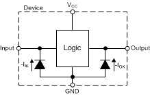
8.3.3 Clamp Diodes
The inputs and outputs to this device have negative clamping diodes.
CAUTION
Avoid any voltage below or above the input or output voltage specified in the Absolute Maximum Ratings. In this event, the current must be limited to the maximum input or output clamp current value indicated in the Absolute Maximum Ratings to avoid damage to the device.
 Figure 3. Electrical Placement of Clamping Diodes for Each Input and Output
8.3.4 Partial Power Down (Ioff)
The inputs and outputs for this device enter a high impedance state when the supply voltage is 0 V. The maximum leakage into or out of any input or output pin on the device is specified by Ioff in the Electrical Characteristics.
8.3.5 Over-voltage Tolerant Inputs
Input signals to this device can be driven above the supply voltage so long as they remain below the maximum input voltage value specified in the Recommended Operating Conditions.
8.4 Function Table
Table 1 lists the functional modes of the SN74LVC1G86 device.
Table 1. Function Table
| INPUTS | OUTPUT Y |
|
|---|---|---|
| A | B | |
| L | L | L |
| L | H | H |
| H | L | H |
| H | H | L |