SCES193N April 1999 – January 2015 SN74LVC2G00
PRODUCTION DATA.
- 1 Features
- 2 Applications
- 3 Description
- 4 Simplified Schematic
- 5 Revision History
- 6 Pin Configuration and Functions
- 7 Specifications
- 8 Parameter Measurement Information
- 9 Detailed Description
- 10Application and Implementation
- 11Power Supply Recommendations
- 12Layout
- 13Device and Documentation Support
- 14Mechanical, Packaging, and Orderable Information
パッケージ・オプション
デバイスごとのパッケージ図は、PDF版データシートをご参照ください。
メカニカル・データ(パッケージ|ピン)
- DCU|8
- YZP|8
- DCT|8
サーマルパッド・メカニカル・データ
発注情報
1 Features
- Available in the Texas Instruments
NanoFree™ Package - Supports 5-V VCC Operation
- Inputs Accept Voltages to 5.5 V
- Max tpd of 4.3 ns at 3.3 V
- Low Power Consumption, 10-μA Max ICC
- ±24-mA Output Drive at 3.3 V
- Typical VOLP (Output Ground Bounce)
< 0.8 V at VCC = 3.3 V, TA = 25°C - Typical VOHV (Output VOH Undershoot)
> 2 V at VCC = 3.3 V, TA = 25°C - Ioff Supports Live Insertion, Partial Power
Down Mode, and Back Drive Protection - Latch-Up Performance Exceeds 100 mA
Per JESD 78, Class II - ESD Protection Exceeds JESD 22
- 2000-V Human-Body Model
- 1000-V Charged-Device Model
2 Applications
- IP Phones: Wired and Wireless
- Optical Modules
- Optical Networking: EPON and Video Over Fiber
- Point-to-Point Microwave Backhaul
- Power: Telecom DC/DC Module:
Analog and Digital - Private Branch Exchanges (PBX)
- TETRA Base Exchanges
- Telecom Base Band Units
- Telecom Shelters: Power Distribution Units (PDU), Power Monitoring Units (PMU), Wireless Battery Monitoring, Remote Electrical Tilt Units (RET), Remote Radio Units (RRU), Tower Mounted Amplifiers (TMA)
- Vector Signal Analyzers and Generators
- Video Conferencing: IP-Based HD
- WiMAX and Wireless Infrastructure Equipment
- Wireless Communications Testers and
Wireless Repeaters - xDSL Modems and DSLAM
3 Description
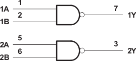
This dual 2-input positive-NAND gate is designed for 1.65-V to 5.5-V VCC operation.
The SN74LVC2G00 device performs the Boolean function Y = A × B or Y = A + B in positive logic.
NanoFree™ package technology is a major breakthrough in IC packaging concepts, using the die as the package.
This device is fully specified for partial-power-down applications using Ioff. The Ioff circuitry disables the outputs, preventing damaging current backflow through the device when it is powered down.
Device Information(1)
| PART NUMBER | PACKAGE | BODY SIZE (NOM) |
|---|---|---|
| SN74LVC2G00 | SM8 (8) | 2.95 mm × 2.80 mm |
| US8 (8) | 2.30 mm × 2.00 mm | |
| DSBGA (8) | 1.91 mm × 0.91 mm |
- For all available packages, see the orderable addendum at the end of the data sheet.
4 Simplified Schematic