SCES770A December 2008 – March 2017 SN74LVC8T245-EP
PRODUCTION DATA.
- 1 Features
- 2 Applications
- 3 Description
- 4 Revision History
- 5 Description (continued)
- 6 Pin Configuration and Functions
-
7 Specifications
- 7.1 Absolute Maximum Ratings
- 7.2 ESD Ratings
- 7.3 Recommended Operating Conditions
- 7.4 Thermal Information PW, DW and RHL
- 7.5 Electrical Characteristics
- 7.6 Switching Characteristics
- 7.7 Switching Characteristics
- 7.8 Switching Characteristics
- 7.9 Switching Characteristics
- 7.10 Operating Characteristics
- 8 Parameter Measurement Information
- 9 Detailed Description
- 10Application and Implementation
- 11Power Supply Recommendations
- 12Layout
- 13Device and Documentation Support
- 14Mechanical, Packaging, and Orderable Information
パッケージ・オプション
メカニカル・データ(パッケージ|ピン)
サーマルパッド・メカニカル・データ
発注情報
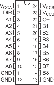
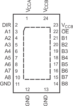
6 Pin Configuration and Functions
PW or DW Package
24-Pin TSSOP or SOIC
(Top View)

RHL Package
24-Pin VQFN
(Top View)

Pin Functions
| PIN | I/O | DESCRIPTION | |
|---|---|---|---|
| NAME | NO. | ||
| A1 | 3 | I/O | Input/output A1. Referenced to VCCA. |
| A2 | 4 | I/O | Input/output A2. Referenced to VCCA. |
| A3 | 5 | I/O | Input/output A3. Referenced to VCCA. |
| A4 | 6 | I/O | Input/output A4. Referenced to VCCA. |
| A5 | 7 | I/O | Input/output A5. Referenced to VCCA. |
| A6 | 8 | I/O | Input/output A6. Referenced to VCCA. |
| A7 | 9 | I/O | Input/output A7. Referenced to VCCA. |
| A8 | 10 | I/O | Input/output A8. Referenced to VCCA. |
| B1 | 21 | I/O | Input/output B1. Referenced to VCCB. |
| B2 | 20 | I/O | Input/output B2. Referenced to VCCB. |
| B3 | 19 | I/O | Input/output B3. Referenced to VCCB. |
| B4 | 18 | I/O | Input/output B4. Referenced to VCCB. |
| B5 | 17 | I/O | Input/output B5. Referenced to VCCB. |
| B6 | 16 | I/O | Input/output B6. Referenced to VCCB. |
| B7 | 15 | I/O | Input/output B7. Referenced to VCCB. |
| B8 | 14 | I/O | Input/output B8. Referenced to VCCB. |
| DIR | 2 | I | Direction-control signal. |
| GND | 11, 12, 13 | G | Ground. |
| OE | 22 | I | Tri-state output-mode enables. Pull OE high to place all outputs in tri-state mode. Referenced to VCCA. |
| VCCA | 1 | P | A-port supply voltage. 1.65 V ≤ VCCA ≤ 5.5 V. |
| VCCB | 23, 24 | P | B-port supply voltage. 1.65 V ≤ VCCA ≤ 5.5 V. |