SCAS319J November 1993 – December 2014 SN74LVCH16652A
PRODUCTION DATA.
- 1 Features
- 2 Applications
- 3 Description
- 4 Simplified Schematic
- 5 Revision History
- 6 Pin Configuration and Functions
-
7 Specifications
- 7.1 Absolute Maximum Ratings
- 7.2 ESD Ratings
- 7.3 Recommended Operating Conditions
- 7.4 Thermal Information
- 7.5 Electrical Characteristics
- 7.6 Timing Requirements, 40°C to 85°C
- 7.7 Timing Requirements, 40°C to 125°C
- 7.8 Switching Characteristics, 40°C to 85°C
- 7.9 Switching Characteristics, 40°C to 125°C
- 7.10 Operating Characteristics
- 7.11 Typical Characteristics
- 8 Parameter Measurement Information
- 9 Detailed Description
- 10Application and Implementation
- 11Power Supply Recommendations
- 12Layout
- 13Device and Documentation Support
- 14Mechanical, Packaging, and Orderable Information
パッケージ・オプション
デバイスごとのパッケージ図は、PDF版データシートをご参照ください。
メカニカル・データ(パッケージ|ピン)
- DGG|56
- DL|56
- DGV|56
サーマルパッド・メカニカル・データ
発注情報
10 Application and Implementation
10.1 Application Information
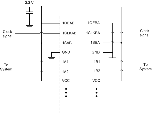
SN74LVCH16652A is a high-drive CMOS device that can be used for a multitude of bus interface type applications where the data needs to be retained or latched. It can produce 24 mA of drive current at 3.3 V, making it Ideal for driving multiple outputs and good for high-speed applications up to 100 MHz. To ensure the high-impedance state during power up or power down, OEBA should be tied to VCC through a pull-up resistor and OEAB should be tied to GND through a pull-down resistor; the minimum value of the resistor is determined by the current-sinking/current-sourcing capability of the driver. Inputs can be driven from either 3.3-V or 5-V devices. This feature allows the use of these devices as translators in a mixed 3.3-V/5-V system environment. Active bus-hold circuitry is provided to hold unused or floating data inputs at a valid logic level. Use of pull-up or pull-down resistors with the bus-hold circuitry is not recommended. The bus-hold circuitry is part of the input circuit and is not disabled by any control pin.
10.2 Typical Application
 Figure 5. Bus-Management Functions
10.2.1 Design Requirements
This device uses CMOS technology and has balanced output drive. Care should be taken to avoid bus contention because it can drive currents that would exceed maximum limits. The high drive will also create fast edges into light loads, so routing and load conditions should be considered to prevent ringing.
10.2.2 Detailed Design Procedure
- Recommended Input Conditions
- For rise time and fall time specifications, see Δt/ΔV in the Recommended Operating Conditions table.
- For specified High and low levels, see VIH and VIL in the Recommended Operating Conditions table.
- Inputs are overvoltage tolerant allowing them to go as high as 5.5 V at any valid VCC.
- Recommend Output Conditions
- Load currents should not exceed 50 mA per output and 100 mA total for the part.
- Outputs should not be pulled above VCC.
10.2.3 Application Curves
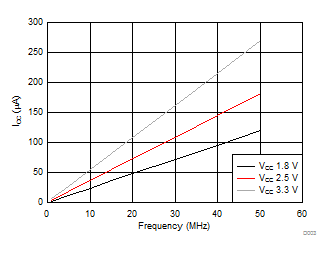
 Figure 6. ICC vs Frequency