JAJSLQ8A September 2021 – December 2021 SN74LXC1T45
PRODUCTION DATA
- 1 特長
- 2 アプリケーション
- 3 概要
- 4 Revision History
- 5 Pin Configuration and Functions
-
6 Specifications
- 6.1 Absolute Maximum Ratings
- 6.2 ESD Ratings
- 6.3 Recommended Operating Conditions
- 6.4 Thermal Information
- 6.5 Electrical Characteristics
- 6.6 Switching Characteristics, VCCA = 1.2 ± 0.1 V
- 6.7 Switching Characteristics, VCCA = 1.5 ± 0.1 V
- 6.8 Switching Characteristics, VCCA = 1.8 ± 0.15 V
- 6.9 Switching Characteristics, VCCA = 2.5 ± 0.2 V
- 6.10 Switching Characteristics, VCCA = 3.3 ± 0.3 V
- 6.11 Switching Characteristics, VCCA = 5.0 ± 0.5 V
- 6.12 スイッチング特性:Tsk、TMAX
- 6.13 Operating Characteristics
- 6.14 Typical Characteristics
- 7 Parameter Measurement Information
-
8 Detailed Description
- 8.1 Overview
- 8.2 Functional Block Diagram
- 8.3
Feature Description
- 8.3.1 CMOS Schmitt-Trigger Inputs with Integrated Pulldowns
- 8.3.2 Balanced High-Drive CMOS Push-Pull Outputs
- 8.3.3 Partial Power Down (Ioff)
- 8.3.4 VCC Isolation and VCC Disconnect (Ioff-float)
- 8.3.5 Over-Voltage Tolerant Inputs
- 8.3.6 Glitch-Free Power Supply Sequencing
- 8.3.7 Negative Clamping Diodes
- 8.3.8 Fully Configurable Dual-Rail Design
- 8.3.9 Supports High-Speed Translation
- 8.4 Device Functional Modes
- 9 Application and Implementation
- 10Power Supply Recommendations
- 11Layout
- 12Device and Documentation Support
- 13Mechanical, Packaging, and Orderable Information
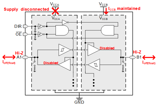
8.3.4 VCC Isolation and VCC Disconnect (Ioff-float)
This device has I/O's with Integrated Dynamic Pull-Down Resistors. The I/O's will get pulled down and then enter a high-impedance state when either supply is < 100 mV or left floating (disconnected), while the other supply is still connected to the device. It is recommended that the I/O's for this device are not driven and kept at a logic low state prior to floating (disconnecting) either supply.
The maximum supply current is specified by ICCx, while VCCx is floating, in the Electrical Characteristics. The maximum leakage into or out of any input or output pin on the device is specified by Ioff(float) in the Electrical Characteristics.
 Figure 8-1 VCC
Disconnect Feature