SDLS144D April 1985 – October 2016 SN54LS240 , SN54LS241 , SN54LS244 , SN54S240 , SN54S241 , SN54S244 , SN74LS240 , SN74LS241 , SN74LS244 , SN74S240 , SN74S241 , SN74S244
- 1 Features
- 2 Applications
- 3 Description
- 4 Revision History
- 5 Pin Configuration and Functions
-
6 Specifications
- 6.1 Absolute Maximum Ratings
- 6.2 ESD Ratings
- 6.3 Recommended Operating Conditions
- 6.4 Thermal Information
- 6.5 Electrical Characteristics - SNx4LS24x
- 6.6 Electrical Characteristics - SNx4S24x
- 6.7 Switching Characteristics - SNx4LS24x
- 6.8 Switching Characteristics - SNx4S24x
- 6.9 Typical Characteristics
- 7 Parameter Measurement Information
- 8 Detailed Description
- 9 Application and Implementation
- 10Power Supply Recommendations
- 11Layout
- 12Device and Documentation Support
- 13Mechanical, Packaging, and Orderable Information
パッケージ・オプション
メカニカル・データ(パッケージ|ピン)
サーマルパッド・メカニカル・データ
発注情報
1 Features
- Inputs Tolerant Down to 2 V, Compatible With
3.3-V or 2.5-V Logic Inputs - Maximum tpd of 15 ns at 5 V
- 3-State Outputs Drive Bus Lines or Buffer Memory Address Registers
- PNP Inputs Reduce DC Loading
- Hysteresis at Inputs Improves Noise Margins
2 Applications
- Servers
- LED Displays
- Network Switches
- Telecom Infrastructure
- Motor Drivers
- I/O Expanders
3 Description
The SNx4LS24x, SNx4S24x octal buffers and line drivers are designed specifically to improve both the performance and density of three-state memory address drivers, clock drivers, and bus-oriented receivers and transmitters. The designer has a choice of selected combinations of inverting and non-inverting outputs, symmetrical, active-low output-control (G) inputs, and complementary output-control (G and G) inputs. These devices feature high fan-out, improved fan-in, and 400-mV noise margin. The SN74LS24x and SN74S24x devices can be used to drive terminated lines down to 133 Ω.
Device Information(1)
| PART NUMBER | PACKAGE | BODY SIZE (NOM) |
|---|---|---|
| SN54LS24x, SN54S24x |
CDIP (20) – J | 24.20 mm × 6.92 mm |
| CFP (20) – W | 7.02 mm × 13.72 mm | |
| LCCC (20) – FK | 8.89 mm × 8.89 mm | |
| SN74LS240, SN74LS244 |
SSOP (20) – DB | 7.20 mm × 5.30 mm |
| SN74LS24x, SN74S24x |
SOIC (20) – DW | 12.80 mm × 7.50 mm |
| PDIP (20) – N | 24.33 mm × 6.35 mm | |
| SN74LS24x | SOP (20) – NS | 7.80 mm × 12.60 mm |
- For all available packages, see the orderable addendum at the end of the data sheet.
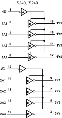
Logic Diagram (Positive Logic)
