SCES625A February 2005 – November 2015 SN74VMEH22501A-EP
PRODUCTION DATA.
- 1 Features
- 2 Applications
- 3 Description
- 4 Revision History
- 5 Description (continued)
- 6 Pin Configuration and Functions
-
7 Specifications
- 7.1 Absolute Maximum Ratings
- 7.2 ESD Ratings
- 7.3 Recommended Operating Conditions
- 7.4 Thermal Information
- 7.5 Electrical Characteristics
- 7.6 Live-Insertion Specifications
- 7.7 Timing Requirements for UBT Transceiver (I Version)
- 7.8 Switching Characteristics for Bus Transceiver Function (I Version)
- 7.9 Switching Characteristics for Bus Transceiver Function (M Version)
- 7.10 Switching Characteristics for UBT Transceiver (I Version)
- 7.11 Switching Characteristics for UBT Transceiver (M Version)
- 7.12 Switching Characteristics for Bus Transceiver Function (I Version)
- 7.13 Switching Characteristics for UBT (I Version)
- 7.14 Switching Characteristics for Bus Transceiver Function (I Version)
- 7.15 Switching Characteristics for UBT (I Version)
- 7.16 Skew Characteristics for Bus Transceiver (I Version)
- 7.17 Skew Characteristics for Bus Transceiver (M Version)
- 7.18 Skew Characteristics for UBT (I Version)
- 7.19 Skew Characteristics for UBT (M Version)
- 7.20 Skew Characteristics for Bus Transceiver (I Version)
- 7.21 Skew Characteristics for UBT (I Version)
- 7.22 Skew Characteristics for Bus Transceiver (I Version)
- 7.23 Skew Characteristics for UBT (I Version)
- 7.24 Maximum Data Transfer Rates
- 7.25 Typical Characteristics
- 8 Parameter Measurement Information
- 9 Detailed Description
- 10Application and Implementation
- 11Power Supply Recommendations
- 12Layout
- 13Device and Documentation Support
- 14Mechanical, Packaging, and Orderable Information
パッケージ・オプション
メカニカル・データ(パッケージ|ピン)
サーマルパッド・メカニカル・データ
発注情報
10 Application and Implementation
NOTE
Information in the following applications sections is not part of the TI component specification, and TI does not warrant its accuracy or completeness. TI’s customers are responsible for determining suitability of components for their purposes. Customers should validate and test their design implementation to confirm system functionality.
10.1 Application Information
Target applications for VME backplanes include industrial controls, telecommunications, simulation, high-energy physics, office automation, and instrumentation systems.
10.2 Typical Application
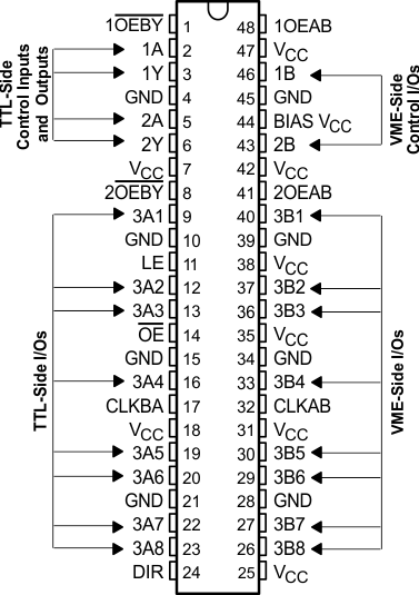 Figure 10. Application Schematic
10.2.1 Design Requirements
The SN74VMEH22501-EP is a combination of 8-bit universal bus transceivers (UBT) and two-bit transceivers, with split LVTTL ports for control and diagnostic monitoring purposes. For the UBTs, 3B1 to 3B8 are the VME-side I/O ports and 3A1 to 3A8 are the LVTTL-side I/O ports. For the two split LVTTL-port transceivers, 1A, 2A are the LVTTL-side input ports, 1Y, 2Y are the LVTTL-side output ports, and 1B, 2B are the VME-side I/O ports (see Figure 5). The UBTs allow transparent, latched, and flip-flop modes of data transfer. It operates at 3.3-V VCC, but can accept 5.5-V input signals at both VME and LVTTL ports. The LVTTL 3A ports and Y outputs have 26-Ω series resistors to reduce the line mismatch on the daughter-card LVTTL side. With the help of Ioff, power-up 3-state, and precharge (BIAS VCC) features, the SN74VMEH22501-EP supports live insertion.
The VME-side input port has tightly controlled input-switching thresholds of ½ VCC ±50 mV for increased noise immunity. In the VMEbus, this input threshold is a clear advantage over the normal TTL or LVTTL type inputs, where VIH(min) is 2.0 V and VIL(max) is 0.8 V. Because the input threshold follows the VCC, data transfer is more immune to the fluctuation of supply voltage, as opposed the ABTE family, where the input threshold is fixed at 1.5 V ±100 mV. To optimize performance, the SN74VMEH22501-EP has been designed into a distributed VME backplane. The OEC™ circuitry, for output edge-rate control, helps reduce reflections as well as electromagnetic interference. The OEC circuitry and high ac drive strength are instrumental in achieving the goal of incident-wave switching. The VME port can source and sink very-high transient currents, which effectively helps to overdrive the reflection on the backplane during transition.
10.2.2 Detailed Design Procedure
By simulating the performance of the device using the VME64x backplane (see Figure 6), the maximum peak current in or out of the B-port output, as the devices switch from one logic state to another, was found to be equivalent to driving the lumped load shown in Figure 11.
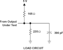 Figure 11. Equivalent AC Peak Output-Current Lumped Load
In general, the rise- and fall-time distribution is shown in Figure 12. Because VME devices were designed for use into distributed loads like the VME64x backplane (B/P), there are significant differences between low-to-high (LH) and high-to-low (HL) values in the lumped load shown in the PMI (see Figure 7 and Figure 8).
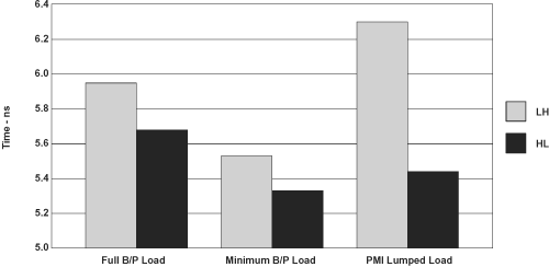 Figure 12. Propagation Delay of VMEH22501 Across Different Loads
10.2.3 Application Curves
Characterization-laboratory data in Figure 13 and Figure 14 show the absolute ac peak output current, with different supply voltages, as the devices change output logic state. A typical nominal process is shown to demonstrate the devices' peak ac output drive capability.
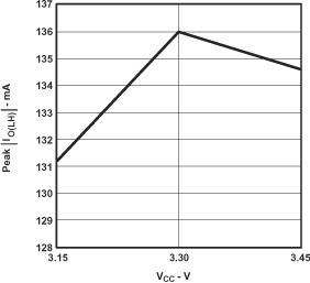 Figure 13. Peak | IO(LH) | vs VCC
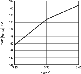 Figure 14. Peak | IO(HL) | vs VCC