JAJSST2D September 1980 – January 2024 SN75157
PRODUCTION DATA
- 1
- 1 特長
- 2 アプリケーション
- 3 概要
- 4 Pin Configuration and Functions
- 5 Specifications
- Parameter Measurement Information
- 6 Detailed Description
- 7 Application and Implementation
- 8 Device and Documentation Support
- 9 Revision History
- 10Mechanical, Packaging, and Orderable Information
パッケージ・オプション
デバイスごとのパッケージ図は、PDF版データシートをご参照ください。
メカニカル・データ(パッケージ|ピン)
- D|8
- P|8
- PS|8
サーマルパッド・メカニカル・データ
- PS|8
発注情報
4 Pin Configuration and Functions
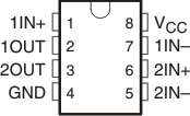
 Figure 4-1 D, P, OR PS Package
(Top View)
Table 4-1 Pin Functions
| PIN | TYPE(1) | DESCRIPTION | |
|---|---|---|---|
| NAME | NO. | ||
| 1IN+ | 1 | I | Non-Inverting Differential Input for Channel 1's Differential Receiver |
| 1OUT | 2 | O | Single Ended Output for Channel 1 Differential Receiver |
| 2OUT | 3 | O | Single Ended Output for Channel 2 Differential Receiver |
| GND | 4 | GND | Device Ground |
| 2IN- | 5 | I | Inverting Differential Input for Channel 2's Differential Receiver |
| 2IN+ | 6 | I | Non-Inverting Differential Input for Channel 2's Differential Receiver |
| 1IN- | 7 | I | Inverting Differential Input for Channel 1's Differential Receiver |
| VCC | 8 | POW | 5V (+/-5%) Positive Supply Connection Pin |
(1) Signal Types: I = Input, O = Output, I/O = Input or Output, POW = Power, GND = Ground.