JAJSUB0C October 1980 – April 2024 SN75172
PRODUCTION DATA
- 1
- 1 特長
- 2 アプリケーション
- 3 概要
- 4 Pin Configuration and Functions
- 5 Specifications
- 6 Parameter Measurement Information
- 7 Detailed Description
- 8 Application and Implementation
- 9 Device and Documentation Support
- 10Revision History
- 11Mechanical, Packaging, and Orderable Information
パッケージ・オプション
デバイスごとのパッケージ図は、PDF版データシートをご参照ください。
メカニカル・データ(パッケージ|ピン)
- N|16
- DW|20
サーマルパッド・メカニカル・データ
発注情報
6 Parameter Measurement Information
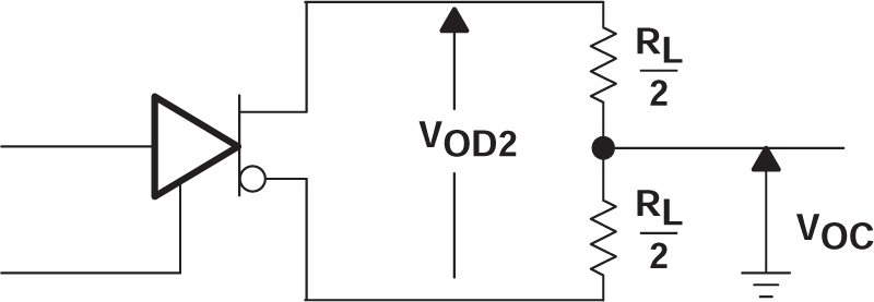
 Figure 6-1 Differential and Common-Mode Output Voltages
A. The
input pulse is supplied by a generator having the following characteristics:
tr ≤ 10ns, tf ≤ 10ns, PRR ≤ 1MHz, duty cycle = 50%,
ZO = 50Ω.
B. CL includes probe and stray capacitance.
Figure 6-2 Differential-Output Test Circuit and Voltage
Waveforms
A. A. The input pulse
is supplied by a generator having the following characteristics: PRR ≤ 1MHz,
duty cycle = 50%, tr ≤ 10ns, tf ≤ 10ns, ZO =
50Ω.
B. CL includes probe and stray capacitance.
C. To test the active-low enable G, ground G and apply an inverted waveform to G.
Figure 6-3 Test Circuit and Voltage Waveforms
A. A. The input pulse
is supplied by a generator having the following characteristics: PRR ≤ 1MHz,
duty cycle = 50%, tr ≤ 5ns, tf ≤ 5ns, ZO =
50Ω.
B. CL includes probe and stray capacitance.
C. To test the active-low enable G, ground G and apply an inverted waveform to G.
Figure 6-4 Test Circuit and Voltage Waveforms