JAJSP93C June 1984 – October 2022 SN75176A
PRODUCTION DATA
- 1 特長
- 2 アプリケーション
- 3 概要
- 4 Revision History
- 5 Pin Configuration and Functions
-
6 Specifications
- 6.1 Absolute Maximum Ratings
- 6.2 Recommended Operating Conditions
- 6.3 Thermal Information
- 6.4 Dissipation Rating Table
- 6.5 Electrical Characteristics – Driver
- 6.6 Electrical Characteristics – Receiver
- 6.7 Switching Characteristics – Driver
- 6.8 Switching Characteristics – Receiver
- 6.9 Typical Characteristics
- 7 Parameter Measurement Information
- 8 Detailed Description
- 9 Application and Implementation
- 10Device and Documentation Support
- 11Mechanical, Packaging, and Orderable Information
パッケージ・オプション
デバイスごとのパッケージ図は、PDF版データシートをご参照ください。
メカニカル・データ(パッケージ|ピン)
- D|8
- P|8
サーマルパッド・メカニカル・データ
発注情報
7 Parameter Measurement Information
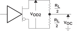
 Figure 7-1 Driver VOD and VOC
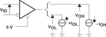
 Figure 7-2 Receiver VOH and VOL
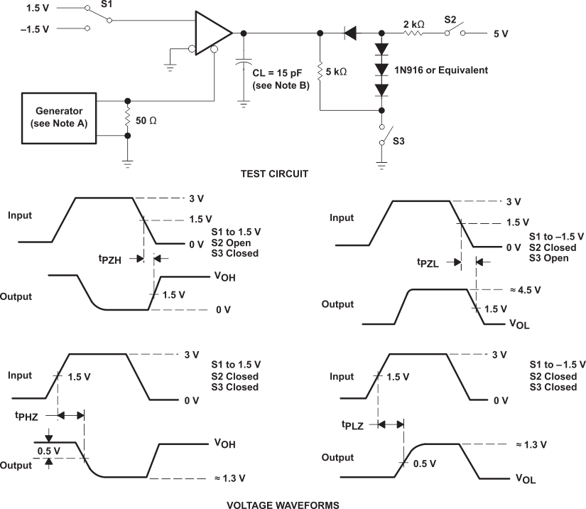
A. The input pulse is supplied
by a generator having the following characteristics: PRR = 1 MHz, 50% duty
cycle, tr ≤ 6 ns, tf ≤ 6 ns, ZO = 50 W.
B. CL includes probe
and jig capacitance.
Figure 7-3 Driver Test Circuit and Voltage Waveforms
A. The input pulse is supplied
by a generator having the following characteristics: PRR = 1 MHz, 50% duty
cycle, tr ≤ 6 ns, tf ≤ 6 ns, ZO = 50 W.
B. CL includes probe
and jig capacitance.
Figure 7-4 Driver Test Circuit and Voltage Waveforms
A. The input pulse is supplied
by a generator having the following characteristics: PRR = 1 MHz, 50% duty
cycle, tr ≤ 6 ns, tf ≤ 6 ns, ZO = 50 W.
B. CL includes probe
and jig capacitance.
Figure 7-5 Driver Test Circuit and Voltage Waveforms
A. The input pulse is supplied
by a generator having the following characteristics: PRR = 1 MHz, 50% duty
cycle, tr ≤ 6 ns, tf ≤ 6 ns, ZO = 50 W.
B. CL includes probe
and jig capacitance.
Figure 7-6 Receiver Test Circuit and Voltage Waveforms
A. The input pulse is supplied
by a generator having the following characteristics: PRR = 1 MHz, 50% duty
cycle, tr ≤ 6 ns, tf ≤ 6 ns, ZO = 50 W.
B. CL includes probe
and jig capacitance.
Figure 7-7 Receiver Test Circuit and voltage Waveforms