JAJSRO6D September 1991 – October 2023 SN75ALS175
PRODUCTION DATA
- 1
- 1 特長
- 2 アプリケーション
- 3 概要
- 4 Pin Configuration and Functions
- 5 Specifications
- 6 Parameter Measurement Information
- 7 Detailed Description
- 8 Device and Documentation Support
- 9 Revision History
- 10Mechanical, Packaging, and Orderable Information
パッケージ・オプション
デバイスごとのパッケージ図は、PDF版データシートをご参照ください。
メカニカル・データ(パッケージ|ピン)
- NS|16
- N|16
サーマルパッド・メカニカル・データ
発注情報
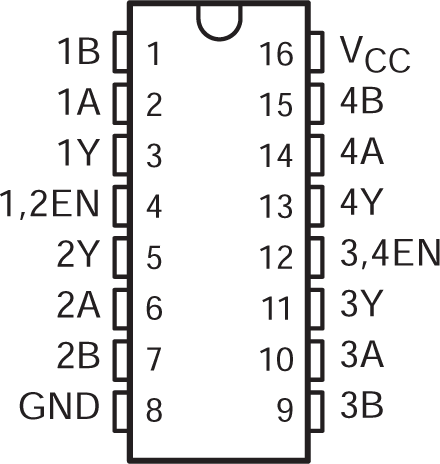
4 Pin Configuration and Functions

A. The NS package is only
available left-end taped and reeled (order device SN75ALS175NSLE).
Figure 4-1 N or NS Package (Top
View)Table 4-1 Pin Functions
| PIN | TYPE(1) | DESCRIPTION | |
|---|---|---|---|
| NAME | NO. | ||
| 1B | 1 | I | Channel 1 Differential Receiver Inverting Input |
| 1A | 2 | I | Channel 1 Differential Receiver Non-Inverting Input |
| 1Y | 3 | O | Channel 1 Single Ended Output |
| G | 4 | I | Active High Enable |
| 2Y | 5 | O | Channel 2 Single Ended Output |
| 2A | 6 | I | Channel 2 Differential Receiver Non-Inverting Input |
| 2B | 7 | I | Channel 2 Differential Receiver Inverting Input |
| GND | 8 | GND | Device GND |
| 3B | 9 | I | Channel 3 Differential Receiver Inverting Input |
| 3A | 10 | I | Channel 3 Differential Receiver Non-Inverting Input |
| 3Y | 11 | O | Channel 3 Single Ended Output |
| G | 12 | I | Active Low Enable |
| 4Y | 13 | O | Channel 4 Single Ended Output |
| 4A | 14 | I | Channel 4 Differential Receiver Non-Inverting Input |
| 4B | 15 | I | Channel 4 Differential Receiver Inverting Input |
| VCC | 16 | PWR | Device VCC (4.75 V to 5.25 V) |
(1) Signal Types: I = Input, O =
Output, I/O = Input or Output.