JAJSTR6E October 1985 – March 2024 SN75ALS194
PRODUCTION DATA
- 1
- 1 特長
- 2 アプリケーション
- 3 概要
- 4 Pin Configuration and Functions
- 5 Specifications
- 6 Parameter Measurement Information
- 7 Detailed Description
- 8 Device and Documentation Support
- 9 Revision History
- 10Mechanical, Packaging, and Orderable Information
パッケージ・オプション
デバイスごとのパッケージ図は、PDF版データシートをご参照ください。
メカニカル・データ(パッケージ|ピン)
- NS|16
- N|16
- D|16
サーマルパッド・メカニカル・データ
発注情報
5.7 Typical Characteristics
Data for temperatures below 0°C and above 70°C are applicable to the SN55ALS194 circuits only.
The A input is connected to VCC during the testing of the Y outputs and to GND during the testing of the Z outputs.
The A input is connected to ground during the testing of the Y outputs and to VCC during the testing of the Z outputs.
 Figure 5-2 Y Output Voltage vs Data Input Voltage
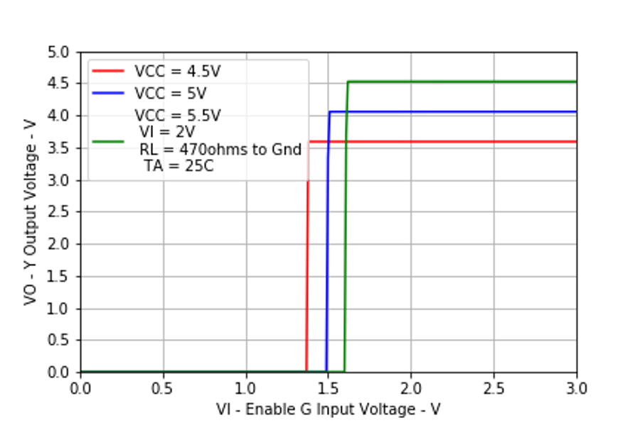 Figure 5-4 Y Output Voltage vs Enable G Input Voltage
 Figure 5-6 Z Output Voltage vs Enable G Input Voltage
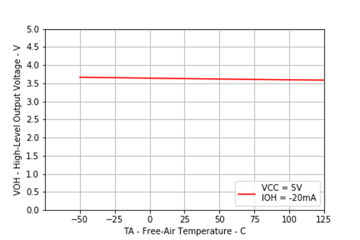 Figure 5-8 High-level Output Voltage vs Free-air Temperature
 Figure 5-10 Low-level Output Voltage vs Free-air Temperature
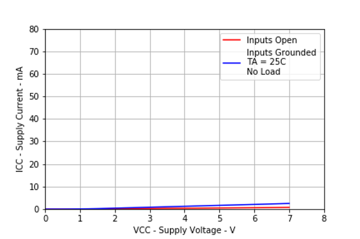 Figure 5-12 Supply Current vs Supply Voltage
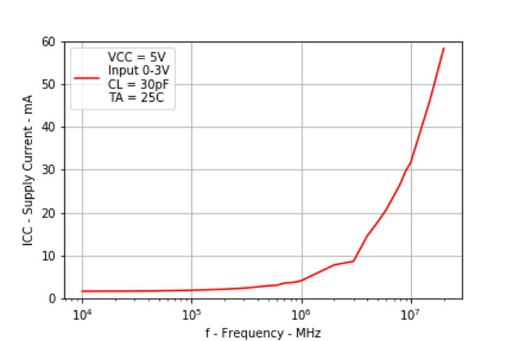 Figure 5-14 Supply Current vs Frequency
 Figure 5-3 Y Output Voltage vs Data Input Voltage
 Figure 5-5 Y Output Voltage vs Enable G Input Voltage
 Figure 5-7 Z Output Voltage vs Enable G Input Voltage
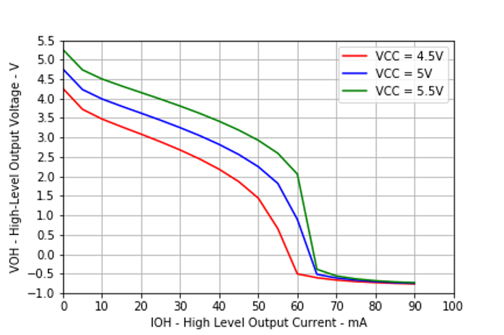 Figure 5-9 High-level Output Voltage vs High-level Output Current
 Figure 5-11 Low-level Output Voltage vs Low-level Output Current
 Figure 5-13 Supply Current vs Supply Voltage