JAJSM53B December 2005 – June 2021 SN65C3232E , SN75C3232E
PRODUCTION DATA
- 1 特長
- 2 アプリケーション
- 3 概要
- 4 Revision History
- 5 Pin Configuration and Functions
-
6 Specifications
- 6.1 Absolute Maximum Ratings
- 6.2 ESD Protection
- 6.3 ESD Protection, Driver
- 6.4 ESD Protection, Receiver
- 6.5 Recommended Operating Conditions
- 6.6 Thermal Information, SN65C3232E
- 6.7 Thermal Information, SN75C3232E
- 6.8 Electrical Characteristics, Power
- 6.9 Electrical Characteristics, Driver
- 6.10 Electrical Characteristics, Receiver
- 6.11 Switching Characteristics, Driver
- 6.12 Switching Characteristics, Receiver
- 7 Parameter Measurement Information
- 8 Detailed Description
- 9 Application and Implenentation
- 10Power Supply Recommendations
- 11Layout
- 12Device and Documentation Support
- 13Mechanical, Packaging, and Orderable Information
パッケージ・オプション
メカニカル・データ(パッケージ|ピン)
サーマルパッド・メカニカル・データ
- DW|16
発注情報
5 Pin Configuration and Functions
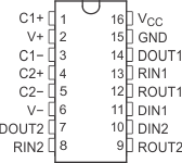
 Figure 5-1 D, DB, DW, or PW Package (Top
View)
Figure 5-1 D, DB, DW, or PW Package (Top
View)Table 5-1 Pin Functions
| PIN | I/O(1) | DESCRIPTION | |
|---|---|---|---|
| NAME | D, DB, DW or PW | ||
| C1+ | 1 | - | Positive lead of C1 capacitor |
| V+ | 2 | O | Positive charge pump output for storage capacitor only |
| C1- | 3 | - | Negative lead of C1 capacitor |
| C2+ | 4 | - | Positive lead of C2 capacitor |
| C2- | 5 | - | Negative lead of C2 capacitor |
| V- | 6 | O | Negative charge pump output for storage capacitor only |
| DOUT2 | 7 | O | RS232 line data output (to remote RS232 system) |
| RIN2 | 8 | I | RS232 line data input (from remote RS232 system) |
| ROUT2 | 9 | O | Logic data output (to UART) |
| DIN2 | 10 | I | Logic data input (from UART) |
| DIN1 | 11 | I | Logic data input (from UART) |
| ROUT1 | 12 | O | Logic data output (to UART) |
| RIN1 | 13 | I | RS232 line data input (from remote RS232 system) |
| DOUT1 | 14 | O | RS232 line data output (to remote RS232 system) |
| GRD | 15 | - | Ground |
| VCC | 16 | - | Supply Voltage, Connect to external 3-V to 5.5-V power supply |
| Thermal Pad | - | - | Exposed thermal pad. Can be connected to GND or left floating. |
(1) Signal Types: I = Input, O = Output, I/O
= Input or Output.