SLLSE57E April 2011 – March 2015 SN75DP130
PRODUCTION DATA.
- 1 Features
- 2 Applications
- 3 Description
- 4 Revision History
- 5 Description (continued)
- 6 Pin Configuration and Functions
- 7 Specifications
- 8 Parameter Measurement Information
- 9 Detailed Description
- 10Application and Implementation
- 11Power Supply Recommendations
- 12Layout
- 13Device and Documentation Support
- 14Mechanical, Packaging, and Orderable Information
パッケージ・オプション
メカニカル・データ(パッケージ|ピン)
- RGZ|48
サーマルパッド・メカニカル・データ
- RGZ|48
発注情報
6 Pin Configuration and Functions
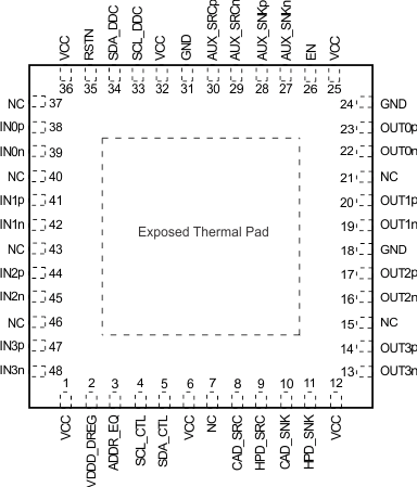
SN75DP130SS RGZ Package
48-Pin VQFN Single Supply
Top View

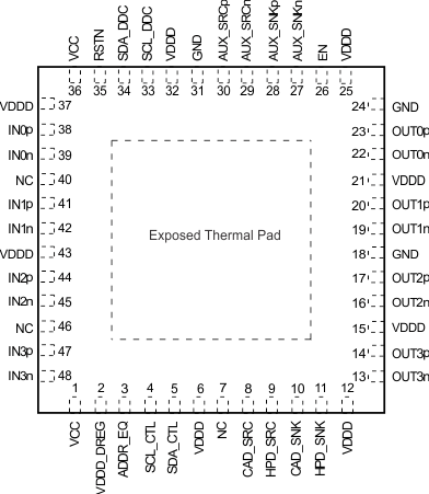
SN75DP130DS RGZ Package
48-Pin VQFN Dual Supply
Top View

Pin Functions
| PIN | I/O | DESCRIPTION | |
|---|---|---|---|
| NAME | NO. | ||
| MAIN LINK TERMINALS | |||
| IN0n | 39 | Input (100-Ω diff) |
DisplayPort Main Link Lane 0 Differential Input |
| IN0p | 38 | ||
| IN1n | 42 | DisplayPort Main Link Lane 1 Differential Input | |
| IN1p | 41 | ||
| IN2n | 45 | DisplayPort Main Link Lane 2 Differential Input | |
| IN2p | 44 | ||
| IN3n | 48 | DisplayPort Main Link Lane 3 Differential Input | |
| IN3p | 47 | ||
| OUT0n | 22 | Output (100-Ω diff) |
DisplayPort Main Link Lane 0 Differential Output |
| OUT0p | 23 | ||
| OUT1n | 19 | DisplayPort Main Link Lane 1 Differential Output | |
| OUT1p | 20 | ||
| OUT2n | 16 | DisplayPort Main Link Lane 2 Differential Output | |
| OUT2p | 17 | ||
| OUT3n | 13 | DisplayPort Main Link Lane 3 Differential Output | |
| OUT3p | 14 | ||
| AUX CHANNEL AND DDC DATA TERMINALS | |||
| AUX_SRCn | 29 | I/O (100-Ω diff) |
Source Side Bidirectional DisplayPort Auxiliary Data Channel. If the AUX_SNK channel is used for monitoring only, these signals are not used and may be left open. |
| AUX_SRCp | 30 | ||
| AUX_SNKn | 27 | I/O (100-Ω diff) |
Sink Side Bidirectional DisplayPort Auxiliary Data Channel. |
| AUX_SNKp | 28 | ||
| SDA_DDC | 34 | I/O | Bidirectional I2C Display Data Channel (DDC) for TMDS mode. These signals may be used together with AUX_SNK to form a FET switch to short-circuit the AC coupling capacitors during TMDS operation in a DP++ Dual-Mode configuration. These terminals include integrated 60-kΩ pullup resistors |
| SCL_DDC | 33 | ||
| HPD, CAD, AND CONTROL TERMINALS | |||
| HPD_SRC | 9 | O | Hot Plug Detect Output to the DisplayPort Source. |
| HPD_SNK | 11 | I | DisplayPort Hot Plug Detect Input from Sink. This device input is 5-V tolerant. |
| Note: Pull this input high during compliance testing or use I2C control interface to go into compliance test mode and control HPD_SNK and HPD_SRC by software. | |||
| CAD_SRC | 8 | O | DP Cable Adapter Detect Output. This output typically drives the GPU CAD input. |
| CAD_SNK | 10 | I | DisplayPort Cable Adapter Detect Input. This input tolerates a 5-V supply with a supply impedance higher than 90kΩ. A device internal zener diode limits the input voltage to 3.3 V. An external 1MΩ resistor to GND is recommended. This terminal is used to select DP mode or TMDS mode in a DP++ Dual-Mode application. |
| SCL_CTL | 4 | I/O | Bidirectional I2C interface to configure the SN75DP130. This interface is active independent of the EN input but inactive when RSTN is low. |
| SDA_CTL | 5 | ||
| RSTN | 35 | I | Active Low Device Reset. This input includes a 150-kΩ resistor to the VDDD core supply. An external capacitor to GND is recommended on the RSTN input to provide a power-up delay (see the VIL and VIH specifications in Recommended Operating Conditions). |
| This signal is used to place the SN75DP130 into Shutdown mode for the lowest power consumption. When the RSTN input is asserted, all outputs (excluding HPD_SRC and CAD_SRC) are high-impedance, and inputs (excluding HPD_SNK and CAD_SNK) are ignored; all I2C and DPCD registers are reset to their default values. | |||
| At power up, the RSTN input must not be de-asserted until the VCC and VDDD supplies have reached at least the minimum recommended supply voltage level (see Figure 34 for timing requirements). | |||
| EN | 26 | I | Device Enable. This input incorporates an internal pullup of 200 kΩ. |
| ADDR_EQ | 3 | 3-level Input | I2C Target Address Select and EQ Configuration Input. If the I2C bus is used, this input setting selects the I2C target address, as described in Figure 19. This input also configures the input EQ to the device, as described in Table 3. |
| SUPPLY AND GROUND TERMINALS | |||
| VDDD | SN75DP130DS
6, 12, 15, 21, 25, 32, 37, 43 |
Digital low voltage core and Main Link supply for SN75DP130DS device option. Nominally 1.1 V. |
|
| VCC | SN75DP130SS
1, 6, 12, 25, 32, 36 |
3.3-V Supply | |
| SN75DP130DS
1, 36 |
|||
| VDDD_DREG | 2 | SN75DP130SS: Digital voltage regulator decoupling; install 1 µF to GND. SN75DP130DS: Treat same as VDDD; this pin will be most noisy of all VDDD terminals and needs a decoupling capacitor nearby. |
|
| GND | 18, 24, 31, and Exposed Thermal Pad |
Ground. Reference GND connections include the device package exposed thermal pad. | |
| NC | SN75DP130SS
7, 15, 21, 37, 40, 43, 46 |
No Connect. These terminals may be left unconnected, or connect to GND. | |
| SN75DP130DS
7, 40, 46 |
|||