JAJSPZ7E november 2002 – march 2023 SN65HVD08 , SN75HVD08
PRODUCTION DATA
- 1 特長
- 2 アプリケーション
- 3 説明
- 4 Revision History
- 5 Pin Configuration and Functions
- 6 Specifications
- 7 Parameter Measurement Information
- 8 Detailed Description
- 9 Application and Implementation
- 10Device and Documentation Support
- 11Mechanical, Packaging, and Orderable Information
パッケージ・オプション
メカニカル・データ(パッケージ|ピン)
サーマルパッド・メカニカル・データ
発注情報
9.1.1 Supply Source Impedance
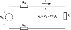
In the steady state, the voltage drop from the source to the load is simply the wire resistance times the load current as modeled in Figure 9-1.
 Figure 9-1 Steady-State Circuit Model
For example, if you were to provide 5-V ±5% supply power to a remote circuit with a maximum load requirement of 0.1 A (one SN65HVD08), the voltage at the load would fall below the 4.5-V minimum of most 5-V circuits with as little as 5.8 m of 28-GA conductors. Table 9-1 summarizes wire resistance and the length for 4.5 V and 3 V at the load with 0.1 A of load current. The maximum lengths would scale linearly for higher or lower load currents.
| WIRE SIZE | RESISTANCE | 4.5-V LENGTH AT 0.1 A | 3-V LENGTH AT 0.1 A |
|---|---|---|---|
| 28 Gauge | 0.213 Ω/m | 5.8 m | 41.1 m |
| 24 Gauge | 0.079 Ω/m | 15.8 m | 110.7 m |
| 22 Gauge | 0.054 Ω/m | 23.1 m | 162.0 m |
| 20 Gauge | 0.034 Ω/m | 36.8 m | 257.3 m |
| 18 Gauge | 0.021 Ω/m | 59.5 m | 416.7 m |
Under dynamic load requirements, the distributed inductance and capacitance of the power lines may not be ignored and decoupling capacitance at the load is required. The amount depends upon the magnitude and frequency of the load current change but, if only powering the SN65HVD08, a 0.1 µF ceramic capacitor is usually sufficient.