JAJSPZ7E november 2002 – march 2023 SN65HVD08 , SN75HVD08
PRODUCTION DATA
- 1 特長
- 2 アプリケーション
- 3 説明
- 4 Revision History
- 5 Pin Configuration and Functions
- 6 Specifications
- 7 Parameter Measurement Information
- 8 Detailed Description
- 9 Application and Implementation
- 10Device and Documentation Support
- 11Mechanical, Packaging, and Orderable Information
パッケージ・オプション
メカニカル・データ(パッケージ|ピン)
サーマルパッド・メカニカル・データ
発注情報
7 Parameter Measurement Information
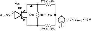
 Figure 7-1 Driver VOD With Common-Mode Loading Test Circuit
 Figure 7-2 Test Circuit and Definitions for the Driver Common-Mode Output Voltage
 Figure 7-3 Driver Switching Test Circuit and Voltage Waveforms
 Figure 7-4 Driver High-Level Enable and Disable Time Test Circuit and Voltage Waveforms
 Figure 7-5 Driver Low-Level Output Enable and Disable Time Test Circuit and Voltage Waveforms
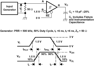
 Figure 7-6 Receiver Switching Test Circuit and Voltage Waveforms
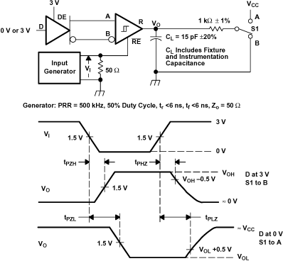
 Figure 7-7 Receiver Enable and Disable Time Test Circuit and Voltage Waveforms With Drivers Enabled
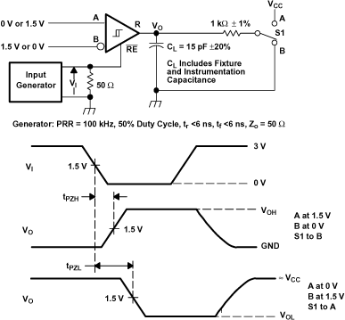
 Figure 7-8 Receiver Enable Time From Standby (Driver Disabled)