SBFS023C June 2003 – December 2016 SRC4190
PRODUCTION DATA.
- 1 Features
- 2 Applications
- 3 Description
- 4 Revision History
- 5 Pin Configuration and Functions
- 6 Specifications
- 7 Detailed Description
-
8 Application and Implementation
- 8.1 Application Information
- 8.2 Typical Application
- 9 Power Supply Recommendations
- 10Layout
- 11Device and Documentation Support
- 12Mechanical, Packaging, and Orderable Information
7 Detailed Description
7.1 Overview
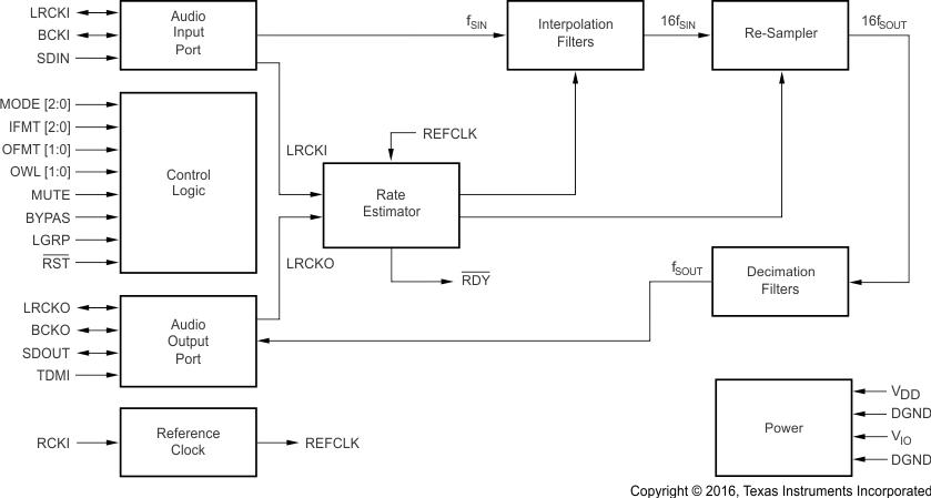
The SRC4190 device is an asynchronous sample rate converter (ASRC) designed for professional audio applications. Operation at input and output sampling frequencies up to 212 kHz is supported, with an input-to-output sampling ratio from 16:1 to 1:16. Excellent dynamic range and total harmonic distortion plus noise (THD+N) are achieved by employing high performance and linear phase digital filtering. Digital filtering options allow for lower group delay processing.
The audio input and output ports support standard audio data formats, as well as a TDM interface mode. 24-,
20-, 18-, and 16-bit word lengths are supported. Both ports may operate in slave mode, deriving their word and bit clocks from external input and output devices. Alternatively, one port may operate in master mode while the other remains in slave mode. In master mode, the LRCK and BCK clocks are derived from the reference clock input (RCKI). The flexible configuration of the input and output ports allows connection to a wide variety of audio data converters, interface devices, digital signal processors, and programmable logic.
A bypass mode is included, which allows audio data to be passed directly from the input port to the output port, bypassing the ASRC function. The bypass option is useful for passing through encoded or compressed audio data, or nonaudio control or status data.
A soft mute function is available providing artifact-free operation while muting the audio output signal. The mute attenuation is typically –128 dB.
The output port data is clocked by either the audio data source in slave mode, or by the SRC4190 in master mode. The input data is passed through interpolation filters which up-sample the data, which is then passed on to the re-sampler. The rate estimator compares the input and output sampling frequencies by comparing LRCKI, LRCKO, and a reference clock. The results include an offset for the FIFO pointer and the coefficients needed for re-sampling function. The output of the re-sampler is then passed on to the decimation filter. The decimation filter performs down-sampling and anti-alias filtering functions.
7.2 Functional Block Diagram
7.3 Feature Description
7.3.1 Soft Mute Function
The soft mute function of the SRC4190 may be invoked by forcing the MUTE pin high. The soft mute function slowly attenuates the output signal level down to all zeroes plus ±4 LSB of dither. This provides an artifact-free muting of the audio output port.
7.3.2 Ready Output
The SRC4190 includes an active low ready output (RDY). This is an output from the rate estimator block, which indicates that the input-to-output sampling frequency ratio has been determined. The ready signal can be used as a flag or indicator output. The ready signal can also be connected to the active high MUTE pin to provide an auto-mute function, so that the output port is muted when the rate estimator is in transition.
7.4 Device Functional Modes
7.4.1 Bypass Mode
The SRC4190 includes a bypass function, which routes the input port data directly to the output port, bypassing the ASRC function. Bypass mode may be invoked by forcing the BYPAS pin high. For normal ASRC operation, the BYPAS pin must be set to 0.
No dithering is applied to the output data in bypass mode; digital attenuation and mute functions are also unavailable in this mode.
7.4.2 Audio Port Modes
The SRC4190 supports seven serial port modes, shown in Table 1. The audio port mode is selected using the MODE0, MODE1, and MODE2 pins.
In slave mode, the port LRCK and BCK clocks are configured as inputs, and receive their clocks from an external audio device. In master mode, the LRCK and BCK clocks are configured as outputs, being derived from the reference clock input (RCKI). Only one port can be set to master mode at any given time, as indicated in Table 1.
Table 1. Setting the Serial Port Modes
| MODE2 | MODE1 | MODE0 | SERIAL PORT MODE |
|---|---|---|---|
| 0 | 0 | 0 | Both input and output ports are slave mode |
| 0 | 0 | 1 | Output port is master mode with RCKI = 128 fS |
| 0 | 1 | 0 | Output port is master mode with RCKI = 512 fS |
| 0 | 1 | 1 | Output port is master mode with RCKI = 256 fS |
| 1 | 0 | 0 | Both input and output ports are slave mode |
| 1 | 0 | 1 | Input port is master mode with RCKI = 128 fS |
| 1 | 1 | 0 | Input port is master mode with RCKI = 512 fS |
| 1 | 1 | 1 | Input port is master mode with RCKI = 256 fS |
7.4.3 Input Port Operation
The audio input port is a three-wire synchronous serial interface that may operate in either slave or master mode. The SDIN pin 4 is the serial audio data input. Audio data is input at this pin in one of three standard audio data formats: Philips I2S, Left Justified, or Right Justified. The audio data word length may be up to 24 bits for I2S and Left Justified formats, while the Right Justified format supports 16, 18, 20, or 24-bit data. The data formats are shown in Figure 59, while critical timing parameters are shown in Figure 60 and listed in Switching Characteristics.
The bit clock is either an input or output at BCKI. In slave mode, BCKI is configured as an input pin, and may operate at rates from 32 fS to 128 fS, with a minimum of one clock cycle per data bit. In master mode, BCKI operates at a fixed rate of 64 fS.
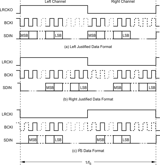 Figure 59. Input Data Formats
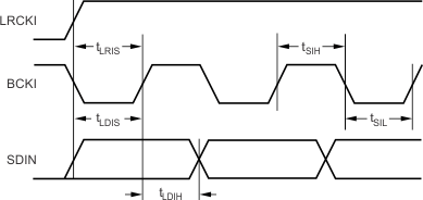 Figure 60. Input Port Timing
The left and right word clock (LRCKI), may be configured as an input or output pin. In slave mode, LRCKI is an input pin, while in master mode LRCKI is an output pin. In either case, the clock rate is equal to the input sampling frequency (fS). The LRCKI duty cycle is fixed to 50% for master mode operation. Table 2 illustrates data format selection for the input port. The IFMT0, IFMT1, and IFMT2 pins are utilized to set the input port data format.
Table 2. Input Port Data Format Selection
| IFMT2 | IMFT1 | IMFT0 | INPUT PORT DATA FORMAT |
|---|---|---|---|
| 0 | 0 | 0 | 24-Bit Left Justified |
| 0 | 0 | 1 | 24-Bit I2S |
| 0 | 1 | 0 | Unused |
| 0 | 1 | 1 | Unused |
| 1 | 0 | 0 | 16-Bit Right Justified |
| 1 | 0 | 1 | 18-Bit Right Justified |
| 1 | 1 | 0 | 20-Bit Right Justified |
| 1 | 1 | 1 | 24-Bit Right Justified |
7.4.4 Output Port Operation
The audio output port is a four-wire synchronous serial interface that may operate in either slave or master mode. The SDOUTpin is the serial audio data output. Audio data is output at this pin in one of four data formats: Philips I2S, Left Justified, Right Justified, or TDM. The audio data word length may be 16, 18, 20, or 24 bits. For all word lengths, the data is triangular PDF dithered from the internal 28-bit data path. The data formats (with the exception of TDM mode) are shown in Figure 61, while critical timing parameters are shown in Figure 62 and listed in Switching Characteristics. The TDM format and timing are shown in Figure 66 and Figure 66, respectively, while examples of standard TDM configurations are shown in Figure 69 and Figure 70. The bit clock is either input or output at BCKO. In slave mode, BCKO is configured as an input pin, and may operate at rates from 32 fS to 128 fS, with a minimum of one clock cycle for each data bit. The exception is the TDM mode, where the BCKO must operate at N × 64fS, where N is equal to the number of SRC4190 devices included on the TDM interface. In master mode, BCKO operates at a fixed rate of 64 fS for all data formats except TDM, where BCKO operates at the reference clock (RCKI) frequency. Additional information regarding TDM mode operation is included in Application and Implementation.
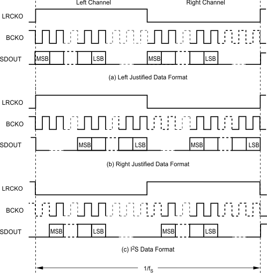 Figure 61. Output Data Formats
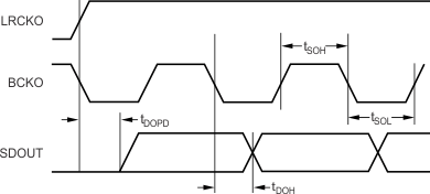 Figure 62. Output Port Timing
The left and right word clock (LRCKO), may be configured as an input or output pin. In slave mode, LRCKO is an input pin, while in master mode it is an output pin. In either case, the clock rate is equal to the output sampling frequency (fS). The clock duty cycle is fixed to 50% for I2S, Left Justified, and Right Justified formats in master mode. The LRCKO pulse width is fixed to 32 BCKO cycles for the TDM format in master mode.
Table 3 shows data format selection for the output port. The OFMT0, OFMT1, OWL0, and OWL1 inputs are utilized to set the output port data format and word length.
Table 3. Output Port Data Format Selection
| OFMT1 | OFMT0 | OUTPUT PORT DATA FORMAT |
|---|---|---|
| 0 | 0 | Left Justified |
| 0 | 1 | I2S |
| 1 | 0 | TDM |
| 1 | 1 | Right Justified |
| OWL1 | OWL2 | OUTPUT PORT DATA WORD LENGTH |
| 0 | 0 | 24 bits |
| 0 | 1 | 20 bits |
| 1 | 0 | 18 bits |
| 1 | 1 | 16 bits |