JAJSNO1A December 2023 – January 2025 TAC5112
PRODUCTION DATA
- 1
- 1 特長
- 2 アプリケーション
- 3 概要
- 4 Device Comparison Table
- 5 Pin Configuration and Functions
-
6 Specifications
- 6.1 Absolute Maximum Ratings
- 6.2 ESD Ratings
- 6.3 Recommended Operating Conditions
- 6.4 Thermal Information
- 6.5 Electrical Characteristics
- 6.6 Timing Requirements: I2C Interface
- 6.7 Switching Characteristics: I2C Interface
- 6.8 Timing Requirements: SPI Interface
- 6.9 Switching Characteristics: SPI Interface
- 6.10 Timing Requirements: TDM, I2S or LJ Interface
- 6.11 Switching Characteristics: TDM, I2S or LJ Interface
- 6.12 Timing Requirements: PDM Digital Microphone Interface
- 6.13 Switching Characteristics: PDM Digital Microphone Interface
- 6.14 Timing Diagrams
- 6.15 Typical Characteristics
-
7 Detailed Description
- 7.1 Overview
- 7.2 Functional Block Diagram
- 7.3
Feature Description
- 7.3.1 Serial Interfaces
- 7.3.2 Phase-Locked Loop (PLL) and Clock Generation
- 7.3.3 Input Channel Configurations
- 7.3.4 Output Channel Configurations
- 7.3.5 Reference Voltage
- 7.3.6 Programmable Microphone Bias
- 7.3.7 Digital PDM Microphone Record Channel
- 7.3.8 Incremental ADC (IADC) Mode
- 7.3.9
Signal-Chain Processing
- 7.3.9.1
ADC Signal-Chain
- 7.3.9.1.1 6 to 4 Input Select Multiplexer (6:4 MUX)
- 7.3.9.1.2 Programmable Channel Gain and Digital Volume Control
- 7.3.9.1.3 Programmable Channel Gain Calibration
- 7.3.9.1.4 Programmable Channel Phase Calibration
- 7.3.9.1.5 Programmable Digital High-Pass Filter
- 7.3.9.1.6 Programmable Digital Biquad Filters
- 7.3.9.1.7 Programmable Channel Summer and Digital Mixer
- 7.3.9.1.8
Configurable Digital Decimation Filters
- 7.3.9.1.8.1
Linear-phase filters
- 7.3.9.1.8.1.1 Sampling Rate: 8kHz or 7.35kHz
- 7.3.9.1.8.1.2 Sampling Rate: 16kHz or 14.7kHz
- 7.3.9.1.8.1.3 Sampling Rate: 24kHz or 22.05kHz
- 7.3.9.1.8.1.4 Sampling Rate: 32kHz or 29.4kHz
- 7.3.9.1.8.1.5 Sampling Rate: 48kHz or 44.1kHz
- 7.3.9.1.8.1.6 Sampling Rate: 96kHz or 88.2kHz
- 7.3.9.1.8.1.7 Sampling Rate: 192kHz or 176.4kHz
- 7.3.9.1.8.2 Low-latency Filters
- 7.3.9.1.8.3 Ultra Low-latency Filters
- 7.3.9.1.8.1
Linear-phase filters
- 7.3.9.1.9 Automatic Gain Controller (AGC)
- 7.3.9.1.10 Voice Activity Detection (VAD)
- 7.3.9.1.11 Ultrasonic Activity Detection (UAD)
- 7.3.9.2
DAC Signal-Chain
- 7.3.9.2.1 Programmable Channel Gain and Digital Volume Control
- 7.3.9.2.2 Programmable Channel Gain Calibration
- 7.3.9.2.3 Programmable Digital High-Pass Filter
- 7.3.9.2.4 Programmable Digital Biquad Filters
- 7.3.9.2.5 Programmable Digital Mixer
- 7.3.9.2.6
Configurable Digital Interpolation Filters
- 7.3.9.2.6.1
Linear-phase filters
- 7.3.9.2.6.1.1 Sampling Rate: 8kHz or 7.35kHz
- 7.3.9.2.6.1.2 Sampling Rate: 16kHz or 14.7kHz
- 7.3.9.2.6.1.3 Sampling Rate: 24kHz or 22.05kHz
- 7.3.9.2.6.1.4 Sampling Rate: 32kHz or 29.4kHz
- 7.3.9.2.6.1.5 Sampling Rate: 48kHz or 44.1kHz
- 7.3.9.2.6.1.6 Sampling Rate: 96kHz or 88.2kHz
- 7.3.9.2.6.1.7 Sampling Rate: 192kHz or 176.4kHz
- 7.3.9.2.6.1.8 Sampling Rate: 384kHz or 352.8kHz
- 7.3.9.2.6.1.9 Sampling Rate 768kHz or 705.6kHz
- 7.3.9.2.6.2 Low-latency Filters
- 7.3.9.2.6.3 Ultra-Low-Latency Filters
- 7.3.9.2.6.1
Linear-phase filters
- 7.3.9.1
ADC Signal-Chain
- 7.3.10 Interrupts, Status, and Digital I/O Pin Multiplexing
- 7.3.11 Power Tune Mode
- 7.4 Device Functional Modes
- 7.5 Programming
-
8 Register Maps
- 8.1 Device Configuration Registers
- 8.2
Programmable Coefficient Registers
- 8.2.1 Programmable Coefficient Registers: Page 8
- 8.2.2 Programmable Coefficient Registers: Page 9
- 8.2.3 Programmable Coefficient Registers: Page 10
- 8.2.4 Programmable Coefficient Registers: Page 11
- 8.2.5 Programmable Coefficient Registers: Page 15
- 8.2.6 Programmable Coefficient Registers: Page 16
- 8.2.7 Programmable Coefficient Registers: Page 17
- 8.2.8 Programmable Coefficient Registers: Page 18
- 8.2.9 Programmable Coefficient Registers: Page 19
- 8.2.10 Programmable Coefficient Registers: Page 25
- 8.2.11 Programmable Coefficient Registers: Page 26
- 8.2.12 Programmable Coefficient Registers: Page 27
- 8.2.13 Programmable Coefficient Registers: Page 28
- 9 Application and Implementation
- 10Device and Documentation Support
- 11Revision History
- 12Mechanical, Packaging, and Orderable Information
7.3.9.1.5 Programmable Digital High-Pass Filter
To remove the DC offset component and attenuate the undesired low-frequency noise content in the record data, the device supports a programmable high-pass filter (HPF). The HPF is not a channel-independent filter setting but is globally applicable for all ADC channels. This HPF is constructed using the first-order infinite impulse response (IIR) filter and is efficient enough to filter out possible DC components of the signal. Table 7-46 shows the predefined –3dB cutoff frequencies available that can be set by using the ADC_DSP_HPF_SEL[1:0] register bits of P0_R114_D[5:4]. Additionally, to achieve a custom –3dB cutoff frequency for a specific application, the device also allows the first-order IIR filter coefficients to be programmed when the HPF_SEL[1:0] register bits are set to 2'b00. Figure 7-28 illustrates the frequency response plot for the HPF filter.
| P0_R114_D[5:4] : ADC_DSP_HPF_SEL[1:0] | -3dB CUTOFF FREQUENCY SETTING | -3dB CUTOFF FREQUENCY AT 16kHz SAMPLE RATE | -3dB CUTOFF FREQUENCY AT 48-kHz SAMPLE RATE |
|---|---|---|---|
| 00 | Programmable 1st-order IIR filter | Programmable 1st-order IIR filter | Programmable 1st-order IIR filter |
| 01 (default) | 0.00002 × fS | 0.25 Hz | 1 Hz |
| 10 | 0.00025 × fS | 4 Hz | 12 Hz |
| 11 | 0.002 × fS | 32 Hz | 96 Hz |
 Figure 7-28 HPF
Filter Frequency Response Plot
Figure 7-28 HPF
Filter Frequency Response PlotEquation 3 gives the transfer function for the first-order programable IIR filter:
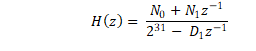
The frequency response for this first-order programmable IIR filter with default coefficients is flat at a gain of 0 dB (all-pass filter). The host device can override the frequency response by programming the IIR coefficients in Table 7-47 to achieve the desired frequency response for high-pass filtering or any other desired filtering. If ADC_DSP_HPF_SEL[1:0] is set to 2'b00, the host device must write these coefficient values for the desired frequency response before powering-up any ADC channel for recording. Table 7-47 shows the filter coefficients for the first-order IIR filter. For additional details on configuring the programmable coefficients, refer Section 8.2.
| FILTER | FILTER COEFFICIENT | DEFAULT COEFFICIENT VALUE | COEFFICIENT REGISTER MAPPING |
|---|---|---|---|
| Programmable 1st-order IIR filter (can be allocated to HPF or any other desired filter) | N0 | 0x7FFFFFFF | P10_R120-R123 |
| N1 | 0x00000000 | P10_R124-R127 | |
| D1 | 0x00000000 | P11_R8-R11 |