JAJSNP5 January   2024 TAC5411-Q1

ADVANCE INFORMATION  

  1.   1
  2. 特長
  3. アプリケーション
  4. 概要
  5. Pin Configuration and Functions
  6. Specifications
    1. 5.1  Absolute Maximum Ratings
    2. 5.2  ESD Ratings
    3. 5.3  Recommended Operating Conditions
    4. 5.4  Thermal Information
    5. 5.5  Electrical Characteristics
    6. 5.6  Timing Requirements: I2C Interface
    7. 5.7  Switching Characteristics: I2C Interface
    8. 5.8  Timing Requirements: SPI Interface
    9. 5.9  Switching Characteristics: SPI Interface
    10. 5.10 Timing Requirements: TDM, I2S or LJ Interface
    11. 5.11 Switching Characteristics: TDM, I2S or LJ Interface
    12. 5.12 Timing Requirements: PDM Digital Microphone Interface
    13. 5.13 Switching Characteristics: PDM Digial Microphone Interface
  7. Detailed Description
    1. 6.1 Overview
    2. 6.2 Functional Block Diagram
    3. 6.3 Feature Description
      1. 6.3.1  Serial Interfaces
        1. 6.3.1.1 Control Serial Interfaces
        2. 6.3.1.2 Audio Serial Interfaces
          1. 6.3.1.2.1 Time Division Multiplexed Audio (TDM) Interface
          2. 6.3.1.2.2 Inter IC Sound (I2S) Interface
          3. 6.3.1.2.3 Left-Justified (LJ) Interface
      2. 6.3.2  Using Multiple Devices With Shared Buses
      3. 6.3.3  Phase-Locked Loop (PLL) and Clock Generation
      4. 6.3.4  Input Channel Configuration
      5. 6.3.5  Reference Voltage
      6. 6.3.6  Microphone Bias
      7. 6.3.7  Input DC Fault Diagnostics
        1. 6.3.7.1 Fault Conditions
          1. 6.3.7.1.1 Input Pin Short to Ground
          2. 6.3.7.1.2 Input Pin Short to MICBIAS
          3. 6.3.7.1.3 Open Inputs
          4. 6.3.7.1.4 Short Between INxP and INxM
          5. 6.3.7.1.5 Input Pin Overvoltage
          6. 6.3.7.1.6 Input Pin Short to VBAT_IN
        2. 6.3.7.2 Fault Reporting
          1. 6.3.7.2.1 Overcurrent and Overtemperature Protection
      8. 6.3.8  Signal-Chain Processing
        1. 6.3.8.1 ADC Signal-Chain
          1. 6.3.8.1.1 Programmable Channel Gain and Digital Volume Control
          2. 6.3.8.1.2 Programmable Channel Gain Calibration
          3. 6.3.8.1.3 Programmable Channel Phase Calibration
          4. 6.3.8.1.4 Programmable Digital High-Pass Filter
          5. 6.3.8.1.5 Programmable Digital Biquad Filters
          6. 6.3.8.1.6 Programmable Channel Summer and Digital Mixer
          7. 6.3.8.1.7 Configurable Digital Decimation Filters
            1. 6.3.8.1.7.1 Linear Phase Filters
              1. 6.3.8.1.7.1.1 Sampling Rate: 16kHz or 14.7kHz
              2. 6.3.8.1.7.1.2 Sampling Rate: 24kHz or 22.05kHz
              3. 6.3.8.1.7.1.3 Sampling Rate: 32kHz or 29.4kHz
              4. 6.3.8.1.7.1.4 Sampling Rate: 48kHz or 44.1kHz
              5. 6.3.8.1.7.1.5 Sampling Rate: 96kHz or 88.2kHz
              6. 6.3.8.1.7.1.6 Sampling Rate: 384kHz or 352.8kHz
      9. 6.3.9  DAC Signal-Chain
        1. 6.3.9.1 Programmable Channel Gain and Digital Volume Control
        2. 6.3.9.2 Programmable Channel Gain Calibration
        3. 6.3.9.3 Programmable Digital High-Pass Filter
        4. 6.3.9.4 Programmable Digital Biquad Filters
        5. 6.3.9.5 Programmable Digital Mixer
        6. 6.3.9.6 Configurable Digital Interpolation Filters
          1. 6.3.9.6.1 Linear Phase Filters
            1. 6.3.9.6.1.1 Sampling Rate: 16kHz or 14.7kHz
            2. 6.3.9.6.1.2 Sampling Rate: 24kHz or 22.05kHz
            3. 6.3.9.6.1.3 Sampling Rate: 32kHz or 29.4kHz
            4. 6.3.9.6.1.4 Sampling Rate: 48kHz or 44.1kHz
            5. 6.3.9.6.1.5 Sampling Rate: 96kHz or 88.2kHz
            6. 6.3.9.6.1.6 Sampling Rate: 384kHz or 352.8kHz
      10. 6.3.10 Interrupts, Status, and Digital I/O Pin Multiplexing
  8. Register Maps
    1. 7.1 Page 0 Registers
    2. 7.2 Page 1 Registers
    3. 7.3 Page_3 Registers
  9. Application and Implementation
    1. 8.1 Application Information
    2. 8.2 Typical Application
      1. 8.2.1 Application
      2. 8.2.2 Design Requirements
      3. 8.2.3 Detailed Design Procedure
  10. Power Supply Recommendations
  11. 10Device and Documentation Support
    1. 10.1 Documentation Support
      1. 10.1.1 Related Documentation
    2. 10.2 ドキュメントの更新通知を受け取る方法
    3. 10.3 サポート・リソース
    4. 10.4 Trademarks
    5. 10.5 静電気放電に関する注意事項
    6. 10.6 用語集
  12. 11Revision History
  13. 12Mechanical, Packaging, and Orderable Information
    1. 12.1 Tape and Reel Information

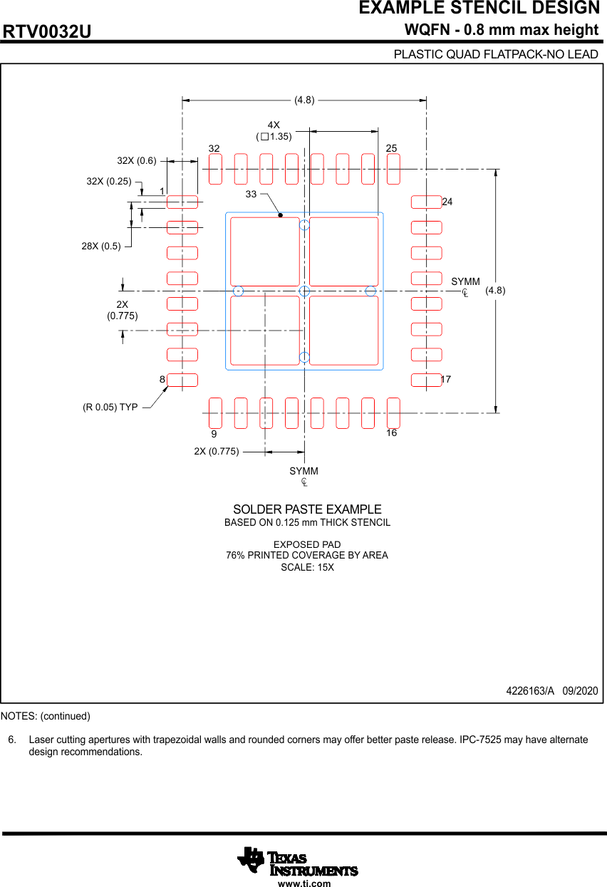
パッケージ・オプション

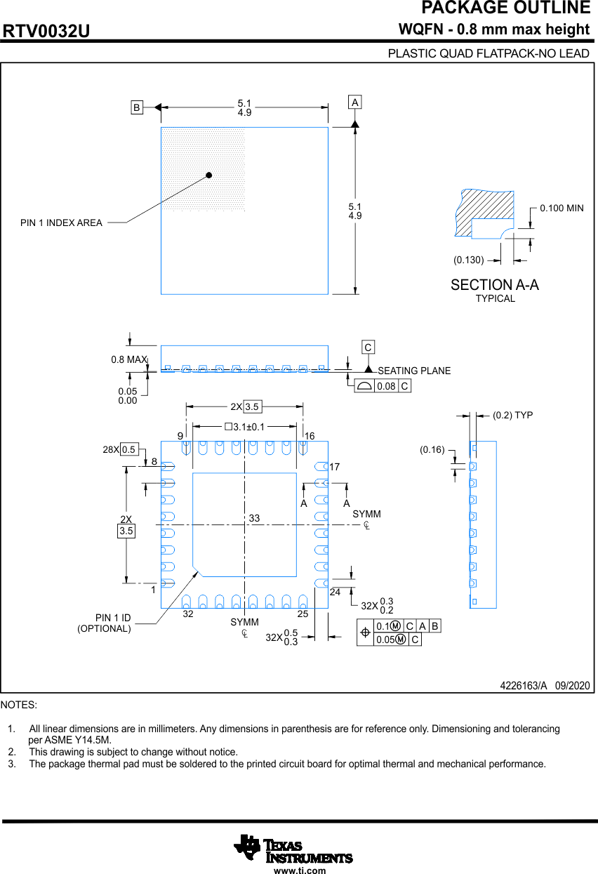
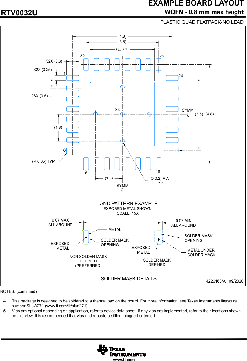
メカニカル・データ(パッケージ|ピン)
サーマルパッド・メカニカル・データ
発注情報

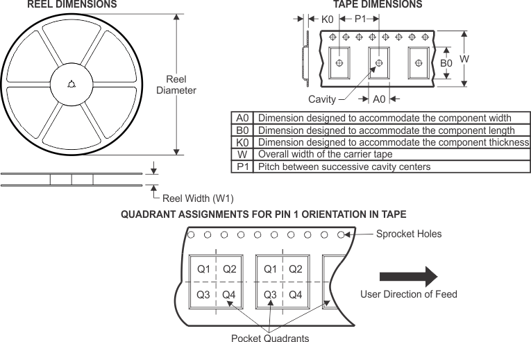
Tape and Reel Information

GUID-DCD52EFC-87A4-47A4-9D04-3D3EAC01766F-low.gif
Device Package
Type
Package Drawing Pins SPQ Reel
Diameter (mm)
Reel
Width W1 (mm)
A0
(mm)
B0
(mm)
K0
(mm)
P1
(mm)
W
(mm)
Pin1
Quadrant
XC5411WQRTVRQ1 WQFN RTV 32 3000 330.0 12.4 5.3 5.3 1.1 8.0 12.0 Q1
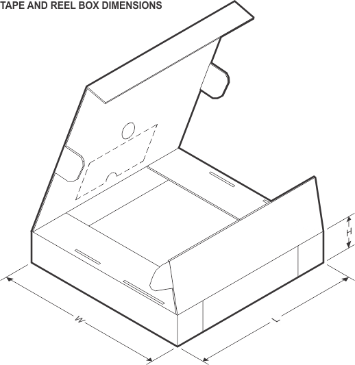
GUID-AC13D00E-1D4D-44B4-9306-767344F9384F-low.gif
Device Package Type Package Drawing Pins SPQ Length (mm) Width (mm) Height (mm)
XC5411WQRTVRQ1 WQFN RTV 32 3000 367.0 367.0 35.0
GUID-20200925-CA0I-6LXZ-LQDK-GKD8LGQ4R7QQ-low.gif
GUID-20200925-CA0I-ZQWT-PQSF-NZ8KRQFWW2RQ-low.gif
GUID-20200925-CA0I-W8M7-ZSHD-JGDMPTVLSFQR-low.gif