JAJSSO0 December 2023 TAD5212
ADVANCE INFORMATION
- 1
- 1 特長
- 2 アプリケーション
- 3 概要
- 4 Revision History
- 5 Pin Configuration and Functions
-
6 Specifications
- 6.1 Absolute Maximum Ratings
- 6.2 ESD Ratings
- 6.3 Recommended Operating Conditions
- 6.4 Thermal Information
- 6.5 Electrical Characteristics
- 6.6 Timing Requirements: I2C Interface
- 6.7 Switching Characteristics: I2C Interface
- 6.8 Timing Requirements: SPI Interface
- 6.9 Switching Characteristics: SPI Interface
- 6.10 Timing Requirements: TDM, I2S or LJ Interface
- 6.11 Switching Characteristics: TDM, I2S or LJ Interface
-
7 Detailed Description
- 7.1 Overview
- 7.2 Functional Block Diagram
- 7.3
Feature Description
- 7.3.1
Serial Interfaces
- 7.3.1.1 Control Serial Interfaces
- 7.3.1.2 Audio Serial Interfaces
- 7.3.1.3 Using Multiple Devices With Shared Buses
- 7.3.1.4 Phase-Locked Loop (PLL) and Clock Generation
- 7.3.1.5 Output Channel Configurations
- 7.3.1.6 Reference Voltage
- 7.3.1.7 Programmable Microphone Bias
- 7.3.1.8
Signal-Chain Processing
- 7.3.1.8.1
DAC Signal-Chain
- 7.3.1.8.1.1 Programmable Channel Gain and Digital Volume Control
- 7.3.1.8.1.2 Programmable Channel Gain Calibration
- 7.3.1.8.1.3 Programmable Digital High-Pass Filter
- 7.3.1.8.1.4 Programmable Digital Biquad Filters
- 7.3.1.8.1.5 Programmable Digital Mixer
- 7.3.1.8.1.6
Configurable Digital Interpolation Filters
- 7.3.1.8.1.6.1
Linear Phase Filters
- 7.3.1.8.1.6.1.1 Sampling Rate: 16 kHz or 14.7 kHz
- 7.3.1.8.1.6.1.2 Sampling Rate: 24 kHz or 22.05 kHz
- 7.3.1.8.1.6.1.3 Sampling Rate: 32 kHz or 29.4 kHz
- 7.3.1.8.1.6.1.4 Sampling Rate: 48 kHz or 44.1 kHz
- 7.3.1.8.1.6.1.5 Sampling Rate: 96 kHz or 88.2 kHz
- 7.3.1.8.1.6.1.6 Sampling Rate: 384 kHz or 352.8 kHz
- 7.3.1.8.1.6.1
Linear Phase Filters
- 7.3.1.8.1
DAC Signal-Chain
- 7.3.1.9 Interrupts, Status, and Digital I/O Pin Multiplexing
- 7.3.1
Serial Interfaces
- 7.4 Device Functional Modes
- 7.5 Register Maps
- 8 Application and Implementation
- 9 Power Supply Recommendations
- 10Device and Documentation Support
- 11Mechanical, Packaging, and Orderable Information
11.1 Tape and Reel Information
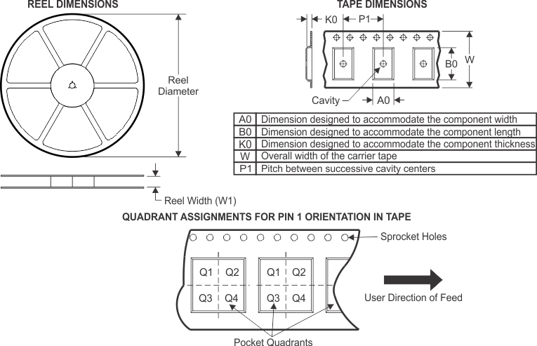
| Device | Package Type |
Package Drawing | Pins | SPQ | Reel Diameter (mm) |
Reel Width W1 (mm) |
A0 (mm) |
B0 (mm) |
K0 (mm) |
P1 (mm) |
W (mm) |
Pin1 Quadrant |
|---|---|---|---|---|---|---|---|---|---|---|---|---|
| XTAD5112IRGER | VQFN | RGE | 24 | 3000 | 330.0 | 12.4 | 4.25 | 4.25 | 1.15 | 8.0 | 12.0 | Q1 |
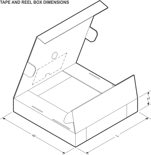
| Device | Package Type | Package Drawing | Pins | SPQ | Length (mm) | Width (mm) | Height (mm) |
|---|---|---|---|---|---|---|---|
| XTAD5112IRGER | VQFN | RGE | 24 | 3000 | 367.0 | 367.0 | 35.0 |


