JAJSDJ0C February 2013 – September 2021 TAS2505
PRODUCTION DATA
- 1 特長
- 2 アプリケーション
- 3 概要
- 4 Revision History
- 5 Pin Configuration and Functions
-
6 Specifications
- 6.1 Absolute Maximum Ratings
- 6.2 ESD Ratings
- 6.3 Recommended Operating Conditions
- 6.4 Thermal Information
- 6.5 Electrical Characteristics
- 6.6 I2S/LJF/RJF Timing in Master Mode
- 6.7 I2S/LJF/RJF Timing in Slave Mode
- 6.8 DSP Timing in Master Mode
- 6.9 DSP Timing in Slave Mode
- 6.10 I2C Interface Timing
- 6.11 SPI Interface Timing
- 6.12 Typical Characteristics
-
7 Detailed Description
- 7.1 Overview
- 7.2 Functional Block Diagram
- 7.3 Feature Description
- 7.4 Device Functional Modes
- 7.5 Register Map
- 8 Application and Implementation
- 9 Power Supply Recommendations
- 10Layout
- 11Device and Documentation Support
- 12Mechanical, Packaging, and Orderable Information
パッケージ・オプション
メカニカル・データ(パッケージ|ピン)
- RGE|24
サーマルパッド・メカニカル・データ
- RGE|24
発注情報
5 Pin Configuration and Functions
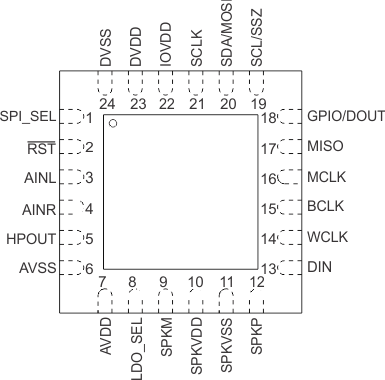
 Figure 5-1 RGE Package24-Pin VQFNTop View
Table 5-1 Pin Functions
| PIN | TYPE(1) | DESCRIPTION | |
|---|---|---|---|
| NO. | NAME | ||
| 1 | SPI_SEL | I | Selects between SPI and I2C digital interface modes; (1 = SPI mode) (0 = I2C mode) |
| 2 | RST | I | Reset for logic, state machines, and digital filters; asserted LOW. |
| 3 | AINL | I | Analog single-ended line left input |
| 4 | AINR | I | Analog single-ended line right input |
| 5 | NC | O | No Connect (Leave unconnected) |
| 6 | AVSS | GND | Analog Ground, 0 V |
| 7 | AVDD | PWR | Analog Core Supply Voltage, 1.5 V to 1.95 V, tied internally to the LDO output |
| 8 | LDO_SEL | I | Select Pin for LDO; ties to either SPKVDD or SPKVSS |
| 9 | SPKM | O | Class-D speaker driver inverting output |
| 10 | SPKVDD | PWR | Class-D speaker driver power supply |
| 11 | SPKVSS | PWR | Class-D speaker driver power supply ground supply |
| 12 | SPKP | O | Class-D speaker driver noninverting output |
| 13 | DIN | I | Audio Serial Data Bus Input Data |
| 14 | WCLK | I/O | Audio Serial Data Bus Word Clock |
| 15 | BCLK | I/O | Audio Serial Data Bus Bit Clock |
| 16 | MCLK | I | Master CLK Input / Reference CLK for CLK Multiplier - PLL (On startup PLLCLK = CLKIN) |
| 17 | MISO | O | SPI Serial Data Output |
| 18 | GPIO/DOUT | I/O/Z | GPIO / Audio Serial Bus Output |
| 19 | SCL/SSZ | I | Either I2C Input Serial Clock or SPI Chip Select Signal depending on SPI_SEL state |
| 20 | SDA/MOSI | I | Either I2C Serial Data Input or SPI Serial Data Input depending on SPI_SEL state. |
| 21 | SCLK | I | Serial clock for SPI interface |
| 22 | IOVDD | PWR | I/O Power Supply, 1.1 V to 3.6 V |
| 23 | DVDD | PWR | Digital Power Supply, 1.65 V to 1.95 V |
| 24 | DVSS | GND | Digital Ground, 0 V |
(1) I = Input, O = Output, GND = Ground, PWR = Power, Z = High
Impedance