SLAS898B January 2014 – April 2015 TAS2552
PRODUCTION DATA.
- 1 Features
- 2 Applications
- 3 Description
- 4 Revision History
- 5 Pin Configuration and Functions
- 6 Specifications
-
7 Detailed Description
- 7.1 Overview
- 7.2 Functional Block Diagram
- 7.3
Feature Description
- 7.3.1 General I2C Operation
- 7.3.2 Single-Byte and Multiple-Byte Transfers
- 7.3.3 Single-Byte Write
- 7.3.4 Multiple-Byte Write and Incremental Multiple-Byte Write
- 7.3.5 Single-Byte Read
- 7.3.6 Multiple-Byte Read
- 7.3.7 PLL
- 7.3.8 Gain Settings
- 7.3.9 Class-D Edge Rate Control
- 7.3.10 Battery Tracking AGC
- 7.3.11 Configurable Boost Current Limit (ILIM)
- 7.4 Device Functional Modes
- 7.5
Register Map
- 7.5.1 Register Map Summary
- 7.5.2 Register 0x00: Device Status Register
- 7.5.3 Register 0x01: Configuration Register 1
- 7.5.4 Register 0x02: Configuration Register 2
- 7.5.5 Register 0x03: Configuration Register 3
- 7.5.6 Register 0x04: DOUT Tristate Mode
- 7.5.7 Register 0x05: Serial Interface Control Register 1
- 7.5.8 Register 0x06: Serial Interface Control Register 2
- 7.5.9 Register 0x07: Output Data Register
- 7.5.10 Register 0x08: PLL Control Register 1
- 7.5.11 Register 0x09: PLL Control Register 2
- 7.5.12 Register 0x0A: PLL Control Register 3
- 7.5.13 Register 0x0B: Battery Tracking Inflection Point Register
- 7.5.14 Register 0x0C: Battery Tracking Slope Control Register
- 7.5.15 Register 0x0D: Reserved Register
- 7.5.16 Register 0x0E: Battery Tracking Limiter Attack Rate and Hysteresis Time
- 7.5.17 Register 0x0F: Battery Tracking Limiter Release Rate
- 7.5.18 Register 0x10: Battery Tracking Limiter Integration Count Control
- 7.5.19 Register 0x11: PDM Configuration Register
- 7.5.20 Register 0x12: PGA Gain Register
- 7.5.21 Register 0x13: Class-D Edge Rate Control Register
- 7.5.22 Register 0x14: Boost Auto-Pass Through Control Register
- 7.5.23 Register 0x15: Reserved Register
- 7.5.24 Register 0x16: Version Number
- 7.5.25 Register 0x17: Reserved Register
- 7.5.26 Register 0x18: Reserved Register
- 7.5.27 Register 0x19: VBAT Data Register
- 8 Applications and Implementation
- 9 Power Supply Recommendations
- 10Layout
- 11Device and Documentation Support
- 12Mechanical, Packaging, and Orderable Information
8 Applications and Implementation
8.1 Application Information
The TAS2552 is a digital or analog input high efficiency Class-D audio power amplifier with advanced battery current management and an integrated Class-G boost converter. In auto passthrough mode, the Class-G boost converter generates the Class-D amplifier supply rail. During low Class-D output power, the boost improves efficiency by deactivating and connecting VBAT directly to the Class-D amplifier supply. When high power audio is required, the boost quickly activates to provide louder audio than a stand-alone amplifier connected directly to the battery. To enable load monitoring, the TAS2552 constantly measures the current and voltage across the load and provides a digital stream of this information back to a processor.
8.2 Typical Applications
8.2.1 Typical Application - Digital Audio Input
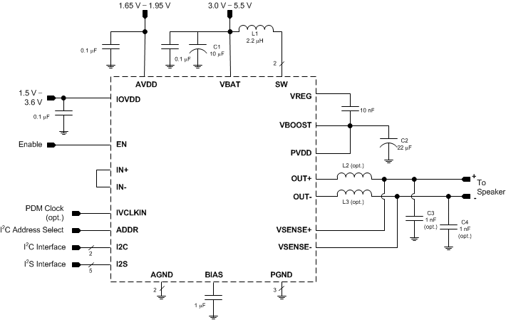 Figure 50. Typical Application Schematic
Table 12. Recommended External Components
| COMPONENT | DESCRIPTION | SPECIFICATION | MIN | TYP | MAX | UNIT |
|---|---|---|---|---|---|---|
| L1 | Boost Converter Inductor | Inductance, 20% Tolerance | 2.2 | µH | ||
| Saturation Current | 2.6 | A | ||||
| L2, L3 | EMI Filter Inductors (optional) | Impedance at 100MHz | 120 | Ω | ||
| DC Resistance | 0.095 | Ω | ||||
| DC Current | 1.5 | A | ||||
| Size | 0402 | EIA | ||||
| C1 | Boost Converter Input Capacitor | Capacitance, 20% Tolerance | 10 | µF | ||
| C2 | Boost Converter Output Capacitor | Type | X5R | |||
| Capacitance, 20% Tolerance | 22 | 47 | µF | |||
| Rated Voltage | 16 | V | ||||
| Capacitance at 8.5 V derating | 7 | µF | ||||
| C3, C4 | EMI Filter Capacitors (optional, must use L2, L3 if C3, C4 used) | Capacitance | 1 | nF |
8.2.1.1 Design Requirements
Table 13. Design Parameters
| DESIGN PARAMETER | EXAMPLE VALUE |
|---|---|
| Audio Input | Digital Audio, I2S |
| Current and Voltage Data Stream | Digital Audio, I2S |
| Mono or Stereo Configuration | Mono |
| Max Output Power at 1% THD+N | 3.3 |
8.2.1.2 Detailed Design Procedure
8.2.1.2.1 Audio Input/Output
The choice of digital or analog audio input is driven by system specific considerations. However, since a digital audio interface will typically be used to send current and voltage data from the TAS2552 to a system processor, using a bidirectional I2S interface is likely to be the best choice.
If a digital audio input is used, the analog inputs, IN+ and IN-, should be shorted together, and not tied to ground.
8.2.1.2.2 Mono/Stereo Configuration
In this application, the device is assumed to be operating in mono mode. See General I2C Operation for information on changing the I2C address of the TAS2552 to support stereo operation. Mono or stereo configuration does not impact the device performance.
8.2.1.2.3 Boost Converter Passive Devices
The boost converter requires three passive devices that are labeled L1, C1 and C2 in Figure 50 and whose specifications are provided in Table 12. These specifications are based on the design of TAS2552 and are necessary to meet the performance targets of the device. In particular, L1 should not be allowed to enter in the current saturation region.
Specifically, the product of L1 and C2 (derated value at 8.5 V) has to be greater than 10e-12 for boost stability after accounting worst case variation of L1 and C2. To satisfy sufficient energy transfer, L1 needs to be > 2 µH at the boost switching frequency (~1.75 MHz). Minimum C2 (derated value at 8.5 V) should be > 4 µF for Class-D power delivery specification. The saturation current for L1 should be > ILIM to deliver Class-D peak power.
8.2.1.2.4 EMI Passive Devices
The TAS2552 supports edge-rate control to minimize EMI, but the system designer may want to include passive devices on the Class-D output devices. These passive devices that are labeled L2, L3, C3 and C4 in Figure 50 and their recommended specifications are provided in Table 12. If C3 and C4 are used, they must be placed after L2 and L3 respectively to maintain the stability of the output stage.
8.2.1.2.5 Miscellaneous Passive Devices
- VREG Capacitor: Needs to be 10 nF to meet boost and class-D power delivery and efficiency specs.
- BIAS Capacitor: Needs to be 1 µF to meet PSSR and noise performance.
8.2.1.3 Application Performance Plots
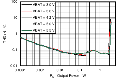
| AGC=OFF, Gain = 15 dB |
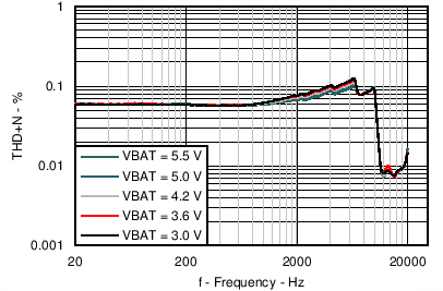
| AGC=OFF, Gain = 15 dB, Pout = 1 W |
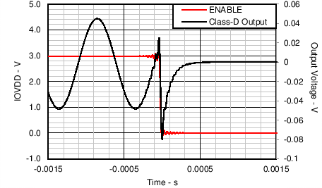
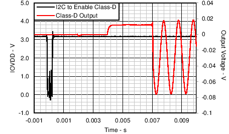
| Class D output and EN pulled low |
8.2.2 Typical Application - Analog Audio Input
Using the analog audio input is very similar to the digital audio input case in Typical Application - Digital Audio Input, and this section will only discuss the differences from the digital input configuration.
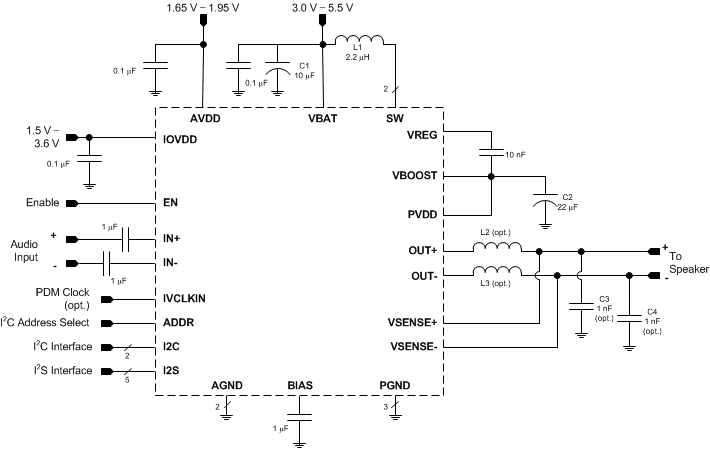 Figure 55. Typical Application Schematic
8.2.2.1 Design Requirements
Table 14. Design Parameters
| DESIGN PARAMETER | EXAMPLE VALUE |
|---|---|
| Audio Input | Analog |
| Current and Voltage Data Stream | Digital Audio, I2S |
| Mono or Stereo Configuration | Mono |
| Max Output Power at 1% THD+N | 3.3 |
8.2.2.2 Detailed Design Procedure
8.2.2.2.1 Audio Input/Output
In this application, system considerations require the use of an analog audio input. Note that a digital audio interface, such as I2S, still needs to be connected to send current and voltage data from the TAS2552 to a system processor.
The analog inputs to TAS2552 should be ac-coupled to the device terminals to allow decoupling of signal source's common mode voltage with that of TAS2552's common mode voltage. The input coupling capacitor in combination with the selected input impedance of TAS2552 forms a high-pass filter.
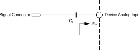 Figure 56. Analog Input Connection
For high fidelity audio playback, it is desirable to keep the cutoff frequency of the high pass filter below the minimum reproducible frequency of the speaker. For example, a 1 µF capacitor connected to the differential analog inputs with input resistance 10 kΩ results in a cutoff frequency of 16 Hz.
8.2.2.3 Application Performance Plots
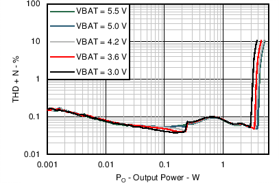
| AGC=OFF, Gain = 15 dB, f = 1 kHz |
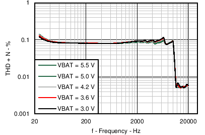
| AGC=OFF, Gain = 15 dB |
8.2.3 Typical Application - Maximum Output Power, Analog Audio Input
This application is the same as Typical Application - Analog Audio Input, except that in this case the boost current limit is set to the maximum value of 3.1 A and the boost inductor needs to be chosen appropriately. See Configurable Boost Current Limit (ILIM) for instructions on setting the boost current limit. The same boost current limit and resulting capacitor change can be used for digital audio input as well.
For schematic, see Figure 55.
Table 15. Recommended External Components
| COMPONENT | DESCRIPTION | SPECIFICATION | MIN | TYP | MAX | UNIT |
|---|---|---|---|---|---|---|
| L1 | Boost Converter Inductor | Inductance, 20% Tolerance | 2.2 | µH | ||
| Saturation Current | 3.1 | A | ||||
| L2, L3 | EMI Filter Inductors (optional) | Impedance at 100MHz | 120 | Ω | ||
| DC Resistance | 0.095 | Ω | ||||
| DC Current | 1.5 | A | ||||
| Size | 0402 | EIA | ||||
| C1 | Boost Converter Input Capacitor | Capacitance, 20% Tolerance | 10 | µF | ||
| C2 | Boost Converter Output Capacitor | Type | X5R | |||
| Capacitance, 20% Tolerance | 22 | 47 | µF | |||
| Rated Voltage | 16 | V | ||||
| Capacitance at 8.5 V derating | 7 | µF | ||||
| C3, C4 | EMI Filter Capacitors (optional, must use L2, L3 if C3, C4 used) | Capacitance | 1 | nF |
8.2.3.1 Design Requirements
Table 16. Design Parameters
| DESIGN PARAMETER | EXAMPLE VALUE |
|---|---|
| Audio Input | Analog |
| Current and Voltage Data Stream | Digital Audio, I2S |
| Mono or Stereo Configuration | Mono |
| Max Output Power at 1% THD+N | 4.0 |
8.2.3.2 Detailed Design Procedure
The Design Procedure is the same as in Detailed Design Procedure.
8.2.3.3 Application Performance Plots
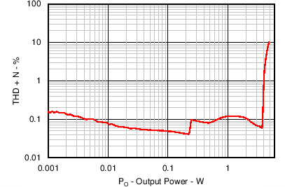
| AGC=OFF, Gain = 15 dB, f = 1 kHz, VBAT = 4.2 V |
8.3 Initialization
To configure the TAS2552, follow these steps.
- Bring-up the power supplies as in Power Supply Sequencing.
- Set the EN terminal to HIGH.
- Configure the registers in the sequence below. Do not set the bits in the final two steps to zero anytime before the end of the sequence.
- Configure device register
- ...
- ...
- ...
- Configure device register
- Set Register 0x0D D[7:0] = 0xC0
- Set Register 0x0E D[5] = 1
- Set Register 0x02 D[0] = 0
- Set Register 0x01 D[1] = 0
