SLES239A November   2008  – December 2016 TAS5352A

PRODUCTION DATA.  

  1. Features
  2. Applications
  3. Description
  4. Revision History
  5. Pin Configuration and Functions
  6. Specifications
    1. 6.1 Absolute Maximum Ratings
    2. 6.2 ESD Ratings
    3. 6.3 Recommended Operating Conditions
    4. 6.4 Thermal Information
    5. 6.5 Electrical Characteristics
    6. 6.6 Audio Specifications (BTL)
    7. 6.7 Audio Specifications (Single-Ended Output)
    8. 6.8 Audio Specifications (PBTL)
    9. 6.9 Typical Characteristics
      1. 6.9.1 BTL Configuration
      2. 6.9.2 SE Configuration
      3. 6.9.3 PBTL Configuration
  7. Detailed Description
    1. 7.1 Overview
    2. 7.2 Functional Block Diagram
    3. 7.3 Feature Description
      1. 7.3.1 System Power-Up and Power-Down Sequence
        1. 7.3.1.1 Powering Up
        2. 7.3.1.2 Powering Down
      2. 7.3.2 Mid Z Sequence Compatibility
      3. 7.3.3 Error Reporting
      4. 7.3.4 Device Protection System
        1. 7.3.4.1 Use of TAS5352A in High-Modulation-Index Capable Systems
        2. 7.3.4.2 Overcurrent (OC) Protection With Current Limiting and Overload Detection
        3. 7.3.4.3 Pin-to-Pin Short-Circuit Protection (PPSC)
        4. 7.3.4.4 Overtemperature Protection
        5. 7.3.4.5 Undervoltage Protection (UVP) and Power-On-Reset (POR)
      5. 7.3.5 Device Reset
    4. 7.4 Device Functional Modes
      1. 7.4.1 Protection MODE Selection Pins
  8. Application and Implementation
    1. 8.1 Application Information
    2. 8.2 Typical Applications
      1. 8.2.1 BTL Application With AD Modulation Filters - 2N
        1. 8.2.1.1 Design Requirements
        2. 8.2.1.2 Detailed Design Procedure
          1. 8.2.1.2.1 PCB Material Recommendation
          2. 8.2.1.2.2 PVDD Capacitor Recommendation
          3. 8.2.1.2.3 Decoupling Capacitor Recommendations
        3. 8.2.1.3 Application Curves
      2. 8.2.2 BTL Application With AD Modulation Filters - 1N
        1. 8.2.2.1 Design Requirements
      3. 8.2.3 SE Application
        1. 8.2.3.1 Design Requirements
        2. 8.2.3.2 Application Curves
      4. 8.2.4 PBTL Application With AD Modulation Filters
        1. 8.2.4.1 Design Requirements
        2. 8.2.4.2 Application Curves
      5. 8.2.5 Non-Differential PBTL Application
        1. 8.2.5.1 Design Requirements
    3. 8.3 System Example
  9. Power Supply Recommendations
  10. 10Layout
    1. 10.1 Layout Guidelines
    2. 10.2 Layout Example
  11. 11Device and Documentation Support
    1. 11.1 Device Support
      1. 11.1.1 Development Support
    2. 11.2 Documentation Support
      1. 11.2.1 Related Documentation
    3. 11.3 Receiving Notification of Documentation Updates
    4. 11.4 Community Resources
    5. 11.5 Trademarks
    6. 11.6 Electrostatic Discharge Caution
    7. 11.7 Glossary
  12. 12Mechanical, Packaging, and Orderable Information

パッケージ・オプション

メカニカル・データ(パッケージ|ピン)
サーマルパッド・メカニカル・データ
発注情報

Layout

Layout Guidelines

  • Use an unbroken ground plane to have good low impedance and inductance return path to the power supply for power and audio signals.
  • Maintain a contiguous ground plane from the ground pins to the PCB area surrounding the device for as many of the ground pins as possible, because the ground pins are the best conductors of heat in the package.
  • PCB layout, audio performance and EMI are linked closely together.
  • Routing the audio input must be kept short and together with the accompanied audio source ground.
  • The small bypass capacitors on the PVDD lines of the DUT be placed as close the PVDD pins as possible.
  • A local ground area underneath the device is important to keep solid to minimize ground bounce.
  • Orient the passive component so that the narrow end of the passive component is facing the TAS5352A device, unless the area between two pads of a passive component is large enough to allow copper to flow in between the two pads.
  • Avoid placing other heat producing components or structures near the TAS5352A device.
  • Avoid cutting off the flow of heat from the TAS5352A device to the surrounding ground areas with traces or via strings, especially on output side of device.

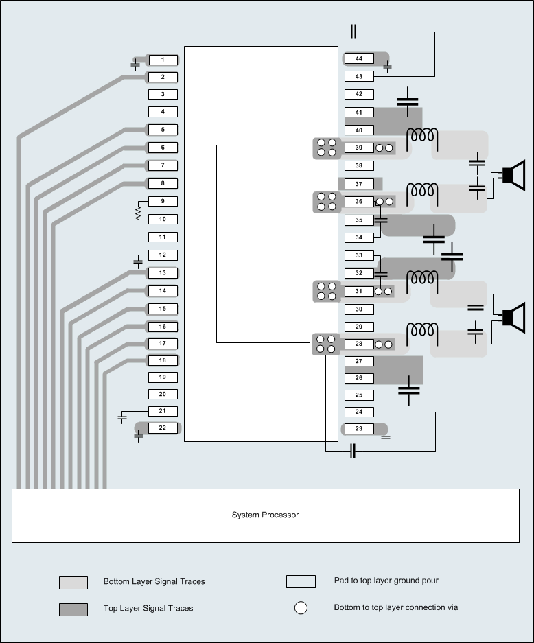
Layout Example

TAS5352A SLES239_layout.gif Figure 20. Layout Recommendation