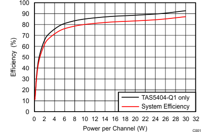
OEM or retail head units where feature densities and system configurations require high efficiency in the audio power amplifier.
The TAS5404-Q1 device is a four-channel class-D audio amplifier designed for use in automotive head units. The TAS5404-Q1 device provides four channels at 20 W continuously into 4 Ω at less than 1% THD+N from a 14.4-Vdc supply when used with the application circuit. The input is configured as an analog single-ended interface. The patented PWM topology of the device provides dramatic improvements in efficiency and audio performance over traditional linear amplifier solutions. The improvement in efficiency and audio performance reduces the power dissipated by the amplifier by a factor of ten under typical music playback conditions. The device incorporates all the required functions required by the OEM application. The built-in load diagnostic functions for detecting and diagnosing disconnected speakers help reduce test time during the manufacturing process.
PART NUMBER | PACKAGE | BODY SIZE (NOM) |
---|---|---|
TAS5404-Q1 | HTQFP (64) | 14.00 mm × 14.00 mm |
Changes from * Revision (August 2015) to A Revision
PART NUMBER | MINIMUM POWER SUPPLY VOLTAGE | MAXIMUM POWER SUPPLY VOLTAGE |
---|---|---|
TAS5404-Q1 | 5.6 VDC | 18 VDC |
TAS5414C-Q1 | 6 VDC | 24 VDC |
NAME | PIN | TYPE(1) | DESCRIPTION |
---|---|---|---|
A_BYP | 11 | PBY | Bypass pin for the AVDD analog regulator |
CLIP_OTW | 6 | DO | Reports CLIP, OTW, or both. Also reports tweeter detection during tweeter mode. Open-drain |
CP | 41 | CP | Top of main storage capacitor for charge pump (bottom goes to PVDD) |
CPC_BOT | 40 | CP | Bottom of flying capacitor for charge pump |
CPC_TOP | 42 | CP | Top of flying capacitor for charge pump |
D_BYP | 5 | PBY | Bypass pin for DVDD regulator output |
FAULT | 1 | DO | Global fault output (open drain): UV, OV, OTSD, OCSD, DC |
GND | 3, 7, 8, 9, 12, 14, 16, 17, 21, 22, 23, 24, 25, 26, 30, 31, 32, 35, 38, 39, 43, 46, 49, 50, 51, 55, 56, 57, 58, 59, 60 | GND | Ground |
I2C_ADDR | 62 | AI | I2C address bit |
IN1_P | 13 | AI | Non-inverting analog input for channel 1 |
IN2_P | 15 | AI | Non-inverting analog input for channel 2 |
IN3_P | 19 | AI | Non-inverting analog input for channel 3 |
IN4_P | 20 | AI | Non-inverting analog input for channel 4 |
IN_M | 18 | ARTN | Signal return for the four analog channel inputs |
MUTE | 2 | AI | Gain ramp control: mute (low), play (high) |
OSC_SYNC | 61 | DI/DO | Oscillator input from master or output to slave amplifiers |
OUT1_M | 48 | PO | – polarity output for bridge 1 |
OUT1_P | 47 | PO | + polarity output for bridge 1 |
OUT2_M | 45 | PO | – polarity output for bridge 2 |
OUT2_P | 44 | PO | + polarity output for bridge 2 |
OUT3_M | 37 | PO | – polarity output for bridge 3 |
OUT3_P | 36 | PO | + polarity output for bridge 3 |
OUT4_M | 34 | PO | – polarity output for bridge 4 |
OUT4_P | 33 | PO | + polarity output for bridge 4 |
PVDD | 27, 28, 29, 52, 53, 54 | PWR | PVDD supply |
REXT | 10 | AI | Precision resistor pin to set analog reference |
SCL | 64 | DI | I2C clock input from system I2C master |
SDA | 63 | DI/DO | I2C data I/O for communication with system I2C master |
STANDBY | 4 | DI | Active-low STANDBY pin. Standby (low), power up (high) |
MIN | MAX | UNIT | |||
---|---|---|---|---|---|
PVDD | DC supply voltage range | Relative to GND | –0.3 | 18 | V |
PVDDMAX | DC supply voltage range | t ≤ 60 s exposure | –0.3 | 30 | V |
PVDDPULSED | Pulsed supply voltage range | t ≤ 100 ms exposure | –1 | 50 | V |
PVDDRAMP | Supply voltage ramp rate | 15 | V/ms | ||
IPVDD | Externally imposed dc supply current per PVDD or GND pin | ±12 | A | ||
IPVDD_MAX | Pulsed supply current per PVDD pin (one shot) | t < 100 ms | 17 | A | |
IO | Maximum allowed DC current per output pin | ±13.5 | A | ||
IO_MAX(1) | Pulsed output current per output pin (single pulse) | t < 100 ms | ±17 | A | |
IIN_MAX | Maximum current, all digital and analog input pins(2) | DC or pulsed | ±1 | mA | |
IMUTE_MAX | Maximum current on MUTE pin | DC or pulsed | ±20 | mA | |
IIN_ODMAX | Maximum sink current for open-drain pins | 7 | mA | ||
VLOGIC | Input voltage range for pin relative to GND (SCL, SDA, I2C_ADDR pins) | Supply voltage range: 6 V < PVDD < 18 V |
–0.3 | 6 | V |
VMUTE | Voltage range for MUTE pin relative to GND | Supply voltage range: 6 V < PVDD < 18 V |
–0.3 | 7.5 | V |
VSTANDBY | Input voltage range for STANDBY pin | Supply voltage range: 6 V < PVDD < 18 V |
–0.3 | 5.5 | V |
VOSC_SYNC | Input voltage range for OSC_SYNC pin relative to GND | Supply voltage range: 6 V < PVDD < 18 V |
–0.3 | 3.6 | V |
VGND | Maximum voltage between GND pins | ±0.3 | V | ||
VAIN_AC_MAX | Maximum ac-coupled input voltage(2), analog input pins | Supply voltage range: 6 V < PVDD < 18 V |
1.9 | Vrms | |
TJ | Maximum operating junction temperature range | –55 | 150 | °C | |
Tstg | Storage temperature | –55 | 150 | °C |
VALUE | UNIT | ||||
---|---|---|---|---|---|
V(ESD) | Electrostatic discharge | Human body model (HBM), per AEC Q100-002(1) | ±2500 | V | |
Charged device model (CDM), per AEC Q100-011 PHD Package | Corner pins excluding SCL | ±750 | V | ||
All pins (including SCL) except CP and CP_Top | ±600 | ||||
CP and CP_Top pins | ±400 |
MIN | NOM | MAX | UNIT | |||
---|---|---|---|---|---|---|
PVDDOP | DC supply voltage range relative to GND | 6 | 14.4 | 18 | V | |
VAIN(2) | Analog audio input signal level (TAS5414C-Q1) | AC-coupled input voltage | 0 | 0.25–1(3) | Vrms | |
TA | Ambient temperature | –40 | 105 | °C | ||
TJ | Junction temperature | An adequate heat sink is required to keep TJ within specified range. | –40 | 115 | °C | |
RL | Nominal speaker load impedance | 2 | 4 | Ω | ||
VPU | Pullup voltage supply (for open-drain logic outputs) | 3 | 3.3 or 5 | 5.5 | V | |
RPU_EXT | External pullup resistor on open-drain logic outputs | Resistor connected between open-drain logic output and VPU supply | 10 | 50 | kΩ | |
RPU_I2C | I2C pullup resistance on SDA and SCL pins | 1 | 4.7 | 10 | kΩ | |
RI2C_ADD | Total resistance of voltage divider for I2C address slave 1 or slave 2, connected between D_BYP and GND pins | 10 | 50 | kΩ | ||
RREXT | External resistance on REXT pin | 1% tolerance required | 19.8 | 20 | 20.2 | kΩ |
CD_BYP , CA_BYP |
External capacitance on D_BYP and A_BYP pins | 10 | 120 | nF | ||
COUT | External capacitance to GND on OUT_X pins | 150 | 680 | nF | ||
CIN | External capacitance to analog input pin in series with input signal | 0.47 | μF | |||
CFLY | Flying capacitor on charge pump | 0.47 | 1 | 1.5 | μF | |
CP | Charge pump capacitor | 50 V required for load dump | 0.47 | 1 | 1.5 | μF |
CMUTE | MUTE pin capacitor | 100 | 220 | 1000 | nF | |
COSCSYNC_MAX | Allowed loading capacitance on OSC_SYNC pin | 75 | pF |
THERMAL METRIC(1) | TAS5404-Q1 | UNIT | |
---|---|---|---|
RθJC | Junction-to-case (heat slug) thermal resistance | 1.2 | °C/W |
RθJA | Junction-to-ambient thermal resistance | This TAS5404-Q1 device is not intended to be used without a heatsink. Therefore, RθJA is not specified. Refer to the Thermal Consideration section. |
PARAMETER | TEST CONDITIONS | MIN | TYP | MAX | UNIT | |
---|---|---|---|---|---|---|
OPERATING CURRENT | ||||||
IPVDD_IDLE | PVDD idle current | All four channels in MUTE mode | 170 | 220 | mA | |
IPVDD_Hi-Z | All four channels in Hi-Z mode | 93 | ||||
IPVDD_STBY | PVDD standby current | STANDBY mode, TJ ≤ 85°C | 2 | 10 | μA | |
OUTPUT POWER | ||||||
POUT | Output power per channel | 4 Ω, THD+N ≤ 1%, 1 kHz, Tc = 75°C | 20 | W | ||
4 Ω, THD+N = 10%, 1 kHz, Tc = 75°C | 25 | 26 | ||||
4 Ω, square wave, 1 kHz, Tc = 75°C | 43 | |||||
2 Ω, THD+N = 1%, 1 kHz, Tc = 75°C | 38 | |||||
2 Ω, THD+N = 10%, 1 kHz, Tc = 75°C | 40 | 45 | ||||
2 Ω, square wave, 1 kHz, Tc = 75°C | 70 | |||||
EFFP | Power efficiency | 4 channels operating, 20-W output power/ch, L = 10 μH, TJ ≤ 85°C | 90% | |||
AUDIO PERFORMANCE | ||||||
VNOISE | Noise voltage at output | Zero input, and A-weighting | 60 | 100 | μV | |
Channel crosstalk | P = 1 W, f = 1 kHz, enhanced crosstalk enabled through I2C (reg. 0x10) | 70 | 85 | dB | ||
CMRR5424 | Common-mode rejection ratio (TAS5424C-Q1) | f = 1 kHz, 1 Vrms referenced to GND, G = 26 dB | 60 | 75 | dB | |
PSRR | Power-supply rejection ratio | PVDD = 14.4 Vdc + 1 Vrms, f = 1 kHz | 60 | 75 | dB | |
THD+N | Total harmonic distortion + noise | P = 1 W, f = 1 kHz | 0.02% | 0.1% | ||
fS | Switching frequency | Switching frequency selectable for AM interference avoidance | 336 | 357 | 378 | kHz |
392 | 417 | 442 | ||||
470 | 500 | 530 | ||||
RAIN | Analog input resistance | Internal shunt resistance on each input pin | 63 | 85 | 106 | kΩ |
VIN_CM | Common-mode input voltage | AC-coupled common-mode input voltage (zero differential input) | 1.3 | Vrms | ||
VCM_INT | Internal common-mode input bias voltage | Internal bias applied to IN_M pin | 3.3 | V | ||
G | Voltage gain (VO/VIN) | Source impedance = 0 Ω, gain measurement taken at 1 W of power per channel | 11 | 12 | 13 | dB |
19 | 20 | 21 | ||||
25 | 26 | 27 | ||||
31 | 32 | 33 | ||||
GCH | Channel-to-channel variation | Any gain commanded | –1 | 0 | 1 | dB |
PWM OUTPUT STAGE | ||||||
RDS(on) | FET drain-to-source resistance | Not including bond wire resistance, TJ = 25°C | 65 | 90 | mΩ | |
VO_OFFSET | Output offset voltage | Zero input signal, G = 26 dB | ±10 | ±50 | mV | |
PVDD OVERVOLTAGE (OV) PROTECTION | ||||||
VOV_SET | PVDD overvoltage shutdown set | 24.6 | 26.4 | 28.2 | V | |
VOV_CLEAR | PVDD overvoltage shutdown clear | 24.4 | 25.9 | 27.4 | V | |
PVDD UNDERVOLTAGE (UV) PROTECTION | ||||||
VUV_SET | PVDD undervoltage shutdown set | 4.9 | 5.3 | 5.5 | V | |
VUV_CLEAR | PVDD undervoltage shutdown clear | 6.2 | 6.6 | 6.9 | V | |
AVDD | ||||||
VA_BYP | A_BYP pin voltage | 6.5 | V | |||
VA_BYP_UV_SET | A_BYP UV voltage | 4.8 | V | |||
VA_BYP_UV_CLEAR | Recovery voltage A_BYP UV | 5.3 | V | |||
DVDD | ||||||
VD_BYP | D_BYP pin voltage | 3.3 | V | |||
POWER-ON RESET (POR) | ||||||
VPOR | PVDD voltage for POR | I2C active above this voltage | 4 | V | ||
VPOR_HY | PVDD recovery hysteresis voltage for POR | 0.1 | V | |||
REXT | ||||||
VREXT | Rext pin voltage | 1.27 | V | |||
CHARGE PUMP (CP) | ||||||
VCPUV_SET | CP undervoltage | 4.8 | V | |||
VCPUV_CLEAR | Recovery voltage for CP UV | 4.9 | V | |||
OVERTEMPERATURE (OT) PROTECTION | ||||||
TOTW1_CLEAR | Junction temperature for overtemperature warning | 96 | 112 | 128 | °C | |
TOTW1_SET / TOTW2_CLEAR |
106 | 122 | 138 | °C | ||
TOTW2_SET / TOTW3_CLEAR |
116 | 132 | 148 | °C | ||
TOTW3_SET / TOTSD_CLEAR |
126 | 142 | 158 | °C | ||
TOTSD | Junction temperature for overtemperature shutdown | 136 | 152 | 168 | °C | |
TFB | Junction temperature for overtemperature foldback | Per channel | 130 | 150 | 170 | °C |
CURRENT LIMITING PROTECTION | ||||||
ILIM | Current limit (load current) | 8.5 | A | |||
OVERCURRENT (OC) SHUTDOWN PROTECTION | ||||||
IMAX | Maximum current (peak output current) | Any short to supply, ground, or other channels | 9.8 | A | ||
TWEETER DETECT | ||||||
ITH_TW | Load-current threshold for tweeter detect | 330 | 445 | 560 | mA | |
ILIM_TW | Load-current limit for tweeter detect | 2.1 | A | |||
STANDBY MODE | ||||||
VIH | STANDBY input voltage for logic-level high | 2 | V | |||
VIL | STANDBY input voltage for logic-level low | 0.7 | V | |||
ISTBY | STANDBY pin current | 0.1 | 0.2 | μA | ||
MUTE MODE | ||||||
GMUTE | Output attenuation | MUTE pin ≤ 0.5 V for 200 ms or I2C Mute Enabled | 100 | dB | ||
DC OFFSET DETECT | ||||||
VTH_DC_TOL | DC offset detect threshold tolerance | 25% | ||||
tDCD | DC offset detect step-response time for four channels | 5.3 | s | |||
CLIP_OTW REPORT | ||||||
VOH_CLIPOTW | CLIP_OTW pin output voltage for logic level high (open-drain logic output) | External 47-kΩ pullup resistor to 3 V to 5.5 V | 2.4 | V | ||
VOL_CLIPOTW | CLIP_OTW pin output voltage for logic level low (open-drain logic output) | 0.5 | V | |||
tDELAY_CLIPDET | CLIP_OTW signal delay when output clipping detected | 20 | μs | |||
FAULT REPORT | ||||||
VOH_FAULT | FAULT pin output voltage for logic-level high (open-drain logic output) | External 47-kΩ pullup resistor to 3 V to 5.5 V | 2.4 | V | ||
VOL_FAULT | FAULT pin output voltage for logic-level low (open-drain logic output) | 0.5 | ||||
OPEN, SHORT DIAGNOSTICS | ||||||
RS2P, RS2G | Maximum resistance to detect a short from OUT pin(s) to PVDD or ground | 200 | Ω | |||
ROPEN_LOAD | Minimum load resistance to detect open circuit | Including speaker wires | 300 | 740 | 1300 | Ω |
RSHORTED_LOAD | Maximum load resistance to detect short circuit | Including speaker wires | 0.5 | 1 | 1.5 | Ω |
I2C ADDRESS DECODER | ||||||
tLATCH_I2CADDR | Time delay to latch I2C address after POR | 300 | μs | |||
VI2C_ADDR | Voltage on I2C_ADDR pin for address 0 | Connect to GND | 0% | 0% | 15% | VD_BYP |
Voltage on I2C_ADDR pin for address 1 | External resistors in series between D_BYP and GND as a voltage divider | 25% | 35% | 45% | ||
Voltage on I2C_ADDR pin for address 2 | 55% | 65% | 75% | |||
Voltage on I2C_ADDR pin for address 3 | Connect to D_BYP | 85% | 100% | 100% | ||
I2C | ||||||
tHOLD_I2C | Power-on hold time before I2C communication | STANDBY high | 1 | ms | ||
fSCL | SCL clock frequency | 400 | kHz | |||
VIH | SCL pin input voltage for logic-level high | RPU_I2C = 5-kΩ pullup, supply voltage = 3.3 V or 5 V | 2.1 | 5.5 | V | |
VIL | SCL pin input voltage for logic-level low | –0.5 | 1.1 | V | ||
VOH | SDA pin output voltage for logic-level high | I2C read, RI2C = 5-kΩ pullup, supply voltage = 3.3 V or 5 V |
2.4 | V | ||
VO | SDA pin output voltage for logic-level low | I2C read, 3-mA sink current | 0.4 | V | ||
VIH | SDA pin input voltage for logic-level high | I2C write, RI2C = 5-kΩ pullup, supply voltage = 3.3 V or 5 V |
2.1 | 5.5 | V | |
VIL | SDA pin input voltage for logic-level low | I2C write, RI2C = 5-kΩ pullup, supply voltage = 3.3 V or 5 V |
–0.5 | 1.1 | V | |
C I | Capacitance for SCL and SDA pins | 10 | pF | |||
OSCILLATOR | ||||||
VOH | OSC_SYNC pin output voltage for logic-level high | I2C_ADDR pin set to MASTER mode | 2.4 | V | ||
VOL | OSC_SYNC pin output voltage for logic-level low | 0.5 | V | |||
VIH | OSC_SYNC pin input voltage for logic-level high | I2C_ADDR pin set to SLAVE mode | 2 | V | ||
VIL | OSC_SYNC pin input voltage for logic-level low | 0.8 | V | |||
fOSC_SYNC | OSC_SYNC pin clock frequency | I2C_ADDR pin set to MASTER mode, fS = 500 kHz | 3.76 | 4 | 4.24 | MHz |
I2C_ADDR pin set to MASTER mode, fS = 417 kHz | 3.13 | 3.33 | 3.63 | |||
I2C_ADDR pin set to MASTER mode, fS = 357 kHz | 2.68 | 2.85 | 3 |
MIN | NOM | MAX | UNIT | ||
---|---|---|---|---|---|
tr | Rise time for both SDA and SCL signals | 300 | ns | ||
tf | Fall time for both SDA and SCL signals | 300 | ns | ||
tw(H) | SCL pulse duration, high | 0.6 | μs | ||
tw(L) | SCL pulse duration, low | 1.3 | μs. | ||
tsu(2) | Setup time for START condition | 0.6 | μs | ||
th(2) | START condition hold time until generation of first clock pulse | 0.6 | μs | ||
tsu(1) | Data setup time | 100 | ns | ||
th(1) | Data hold time | 0(1) | ns | ||
tsu(3) | Setup time for STOP condition | 0.6 | μs | ||
CB | Load capacitance for each bus line | 400 | pF |