JAJSG81B December   2015  – September 2018 TAS5411-Q1

PRODUCTION DATA.  

  1. 特長
  2. アプリケーション
  3. 概要
    1.     Device Images
      1.      ブロック概略図
      2.      効率
  4. 改訂履歴
  5. Device Comparison Table
  6. Pin Configuration and Functions
    1.     Pin Functions
  7. Specifications
    1. 7.1 Absolute Maximum Ratings
    2. 7.2 ESD Ratings
    3. 7.3 Recommended Operating Conditions
    4. 7.4 Thermal Information
    5. 7.5 Electrical Characteristics
    6. 7.6 Timing Requirements for I2C Interface Signals
    7. 7.7 Typical Characteristics
  8. Parameter Measurement Information
  9. Detailed Description
    1. 9.1 Overview
    2. 9.2 Functional Block Diagram
    3. 9.3 Feature Description
      1. 9.3.1 Analog Audio Input and Preamplifier
      2. 9.3.2 Pulse-Width Modulator (PWM)
      3. 9.3.3 Gate Drive
      4. 9.3.4 Power FETs
      5. 9.3.5 Load Diagnostics
        1. 9.3.5.1 Load Diagnostics Sequence
        2. 9.3.5.2 Faults During Load Diagnostics
      6. 9.3.6 Protection and Monitoring
      7. 9.3.7 I2C Serial Communication Bus
        1. 9.3.7.1 I2C Bus Protocol
        2. 9.3.7.2 Random Write
        3. 9.3.7.3 Random Read
        4. 9.3.7.4 Sequential Read
    4. 9.4 Device Functional Modes
      1. 9.4.1 Hardware Control Pins
      2. 9.4.2 EMI Considerations
      3. 9.4.3 Operating Modes and Faults
    5. 9.5 Register Maps
  10. 10Application and Implementation
    1. 10.1 Application Information
    2. 10.2 Typical Application
      1. 10.2.1 Design Requirements
        1. 10.2.1.1 Amplifier Output Filtering
        2. 10.2.1.2 Amplifier Output Snubbers
        3. 10.2.1.3 Bootstrap Capacitors
        4. 10.2.1.4 Analog Audio Input Filter
      2. 10.2.2 Detailed Design Procedure
        1. 10.2.2.1 Unused Pin Connections
          1. 10.2.2.1.1 MUTE Pin
          2. 10.2.2.1.2 STANDBY Pin
          3. 10.2.2.1.3 I2C Pins (SDA and SCL)
          4. 10.2.2.1.4 Terminating Unused Outputs
          5. 10.2.2.1.5 Using a Single-Ended Audio Input
      3. 10.2.3 Application Curves
  11. 11Power Supply Recommendations
  12. 12Layout
    1. 12.1 Layout Guidelines
    2. 12.2 Layout Examples
      1. 12.2.1 Top Layer
      2. 12.2.2 Second Layer – Signal Layer
      3. 12.2.3 Third Layer – Power Layer
      4. 12.2.4 Bottom Layer – Ground Layer
  13. 13デバイスおよびドキュメントのサポート
    1. 13.1 デバイス・サポート
      1. 13.1.1 デベロッパー・ネットワークの製品に関する免責事項
    2. 13.2 ドキュメントのサポート
      1. 13.2.1 関連資料
    3. 13.3 ドキュメントの更新通知を受け取る方法
    4. 13.4 コミュニティ・リソース
    5. 13.5 商標
    6. 13.6 静電気放電に関する注意事項
    7. 13.7 Glossary
  14. 14メカニカル、パッケージ、および注文情報

パッケージ・オプション

メカニカル・データ(パッケージ|ピン)
サーマルパッド・メカニカル・データ
発注情報

Timing Requirements for I2C Interface Signals

over recommended operating conditions (unless otherwise noted)
MIN NOM MAX UNIT
f(SCL) SCL clock frequency 400 kHz
tr Rise time for both SDA and SCL signals 300 ns
tf Fall time for both SDA and SCL signals 300 ns
tw(H) SCL pulse duration, high 0.6 μs
tw(L) SCL pulse duration, low 1.3 μs
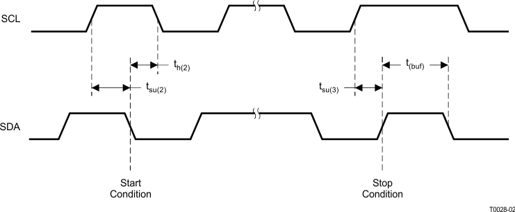
tsu(2) Setup time for START condition 0.6 μs
th(2) START condition hold time before generation of first clock pulse 0.6 μs
tsu(1) Data setup time 100 ns
th(1) Data hold time 0(1) ns
tsu(3) Setup time for STOP condition 0.6 μs
C(B) Load capacitance for each bus line 400 pF
A device must internally provide a hold time of at least 300 ns for the SDA signal to bridge the undefined region of the falling edge of SCL.
TAS5411-Q1 T0027-03_SLOS814.gifFigure 1. SCL and SDA Timing
TAS5411-Q1 T0028-02_SLOS814.gifFigure 2. Timing for Start and Stop Conditions