SLOS795F September 2013 – October 2017 TAS5414C-Q1
PRODUCTION DATA.
- 1 Features
- 2 Applications
- 3 Description
- 4 Revision History
- 5 Pin Configuration and Functions
- 6 Specifications
- 7 Detailed Description
- 8 Application and Implementation
- 9 Power Supply Recommendations
- 10Layout
- 11Device and Documentation Support
- 12Mechanical, Packaging, and Orderable Information
パッケージ・オプション
デバイスごとのパッケージ図は、PDF版データシートをご参照ください。
メカニカル・データ(パッケージ|ピン)
- PHD|64
サーマルパッド・メカニカル・データ
- PHD|64
発注情報
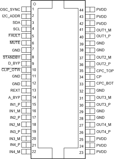
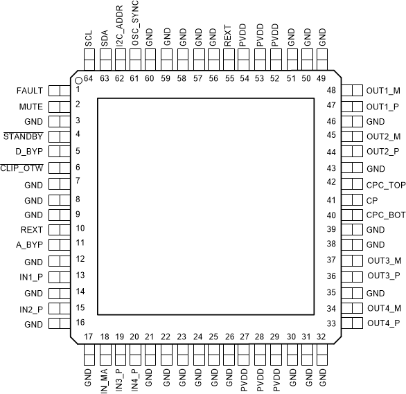
5 Pin Configuration and Functions
DKE Package
(Top View)

Pin Functions
| PIN | TYPE(1) | DESCRIPTION | ||
|---|---|---|---|---|
| NAME | DKE PACKAGE | PHD PACKAGE | ||
| TAS5424C-Q1 NO. |
TAS5414C-Q1 NO. |
|||
| A_BYP | 14 | 11 | PBY | Bypass pin for the AVDD analog regulator |
| CLIP_OTW | 10 | 6 | DO | Reports CLIP, OTW, or both. It also reports tweeter detection during tweeter mode. Open-drain |
| CP | 34 | 41 | CP | Top of main storage capacitor for charge pump (bottom goes to PVDD) |
| CPC_BOT | 33 | 40 | CP | Bottom of flying capacitor for charge pump |
| CPC_TOP | 35 | 42 | CP | Top of flying capacitor for charge pump |
| D_BYP | 9 | 5 | PBY | Bypass pin for DVDD regulator output |
| FAULT | 5 | 1 | DO | Global fault output (open drain): UV, OV, OTSD, OCSD, DC |
| GND | 7, 11, 12, 28, 29, 32, 38, 39 | 3, 7, 8, 9, 12, 14, 16, 17, 21, 22, 23, 24, 25, 26, 30, 31, 32, 35, 38, 39, 43, 46, 49, 50, 51, 55, 56, 57, 58, 59, 60 | GND | Ground |
| I2C_ADDR | 2 | 62 | AI | I2C address bit |
| IN1_M | 16 | N/A | AI | Inverting analog input for channel 1 (TAS5424C-Q1 only) |
| IN1_P | 15 | 13 | AI | Non-inverting analog input for channel 1 |
| IN2_M | 18 | N/A | AI | Inverting analog input for channel 2 (TAS5424C-Q1 only) |
| IN2_P | 17 | 15 | AI | Non-inverting analog input for channel 2 |
| IN3_M | 20 | N/A | AI | Inverting analog input for channel 3 (TAS5424C-Q1 only) |
| IN3_P | 19 | 19 | AI | Non-inverting analog input for channel 3 |
| IN4_M | 22 | N/A | AI | Inverting analog input for channel 4 (TAS5424C-Q1 only) |
| IN4_P | 21 | 20 | AI | Non-inverting analog input for channel 4 |
| IN_M | N/A | 18 | ARTN | Signal return for the four analog channel inputs (TAS5414C-Q1 only) |
| MUTE | 6 | 2 | AI | Gain ramp control: mute (low), play (high) |
| OSC_SYNC | 1 | 61 | DI/DO | Oscillator input from master or output to slave amplifiers |
| OUT1_M | 41 | 48 | PO | – polarity output for bridge 1 |
| OUT1_P | 40 | 47 | PO | + polarity output for bridge 1 |
| OUT2_M | 37 | 45 | PO | – polarity output for bridge 2 |
| OUT2_P | 36 | 44 | PO | + polarity output for bridge 2 |
| OUT3_M | 31 | 37 | PO | – polarity output for bridge 3 |
| OUT3_P | 30 | 36 | PO | + polarity output for bridge 3 |
| OUT4_M | 27 | 34 | PO | – polarity output for bridge 4 |
| OUT4_P | 26 | 33 | PO | + polarity output for bridge 4 |
| PVDD | 23, 24, 25, 42, 43, 44 | 27, 28, 29, 52, 53, 54 | PWR | PVDD supply |
| REXT | 13 | 10 | AI | Precision resistor pin to set analog reference |
| SCL | 4 | 64 | DI | I2C clock input from system I2C master |
| SDA | 3 | 63 | DI/DO | I2C data I/O for communication with system I2C master |
| STANDBY | 8 | 4 | DI | Active-low STANDBY pin. Standby (low), power up (high) |
(1) DI = digital input, DO = digital output, AI = analog input, ARTN = analog signal return, PWR = power supply, PBY = power bypass, PO = power output, GND = ground, CP = charge pump.
