JAJSE39 October 2017 TAS5634
PRODUCTION DATA.
- 1 特長
- 2 アプリケーション
- 3 概要
- 4 改訂履歴
- 5 Device Comparison
- 6 Pin Configuration and Functions
- 7 Specifications
-
8 Detailed Description
- 8.1 Overview
- 8.2 Functional Block Diagrams
- 8.3
Feature Description
- 8.3.1 Closed-Loop Architecture
- 8.3.2 Power Supplies
- 8.3.3 System Power-Up / Power-Down Sequence
- 8.3.4 Startup and Shutdown Ramp Sequence (C_START)
- 8.3.5 Device Protection System
- 8.3.6 Overload and Short Circuit Current Protection
- 8.3.7 DC Speaker Protection
- 8.3.8 Pin-To-Pin Short Circuit Protection (PPSC)
- 8.3.9 Overtemperature Protection
- 8.3.10 Overtemperature Warning, OTW
- 8.3.11 Undervoltage Protection (UVP) and Power-On Reset (POR)
- 8.3.12 Error Reporting
- 8.3.13 Fault Handling
- 8.3.14 System Design Consideration
- 8.4 Device Functional Modes
- 9 Application and Implementation
- 10Power Supply Recommendations
- 11Layout
- 12デバイスおよびドキュメントのサポート
- 13メカニカル、パッケージ、および注文情報
パッケージ・オプション
メカニカル・データ(パッケージ|ピン)
- DDV|44
サーマルパッド・メカニカル・データ
- DDV|44
発注情報
9 Application and Implementation
NOTE
Information in the following applications sections is not part of the TI component specification, and TI does not warrant its accuracy or completeness. TI’s customers are responsible for determining suitability of components for their purposes. Customers should validate and test their design implementation to confirm system functionality.
9.1 Application Information
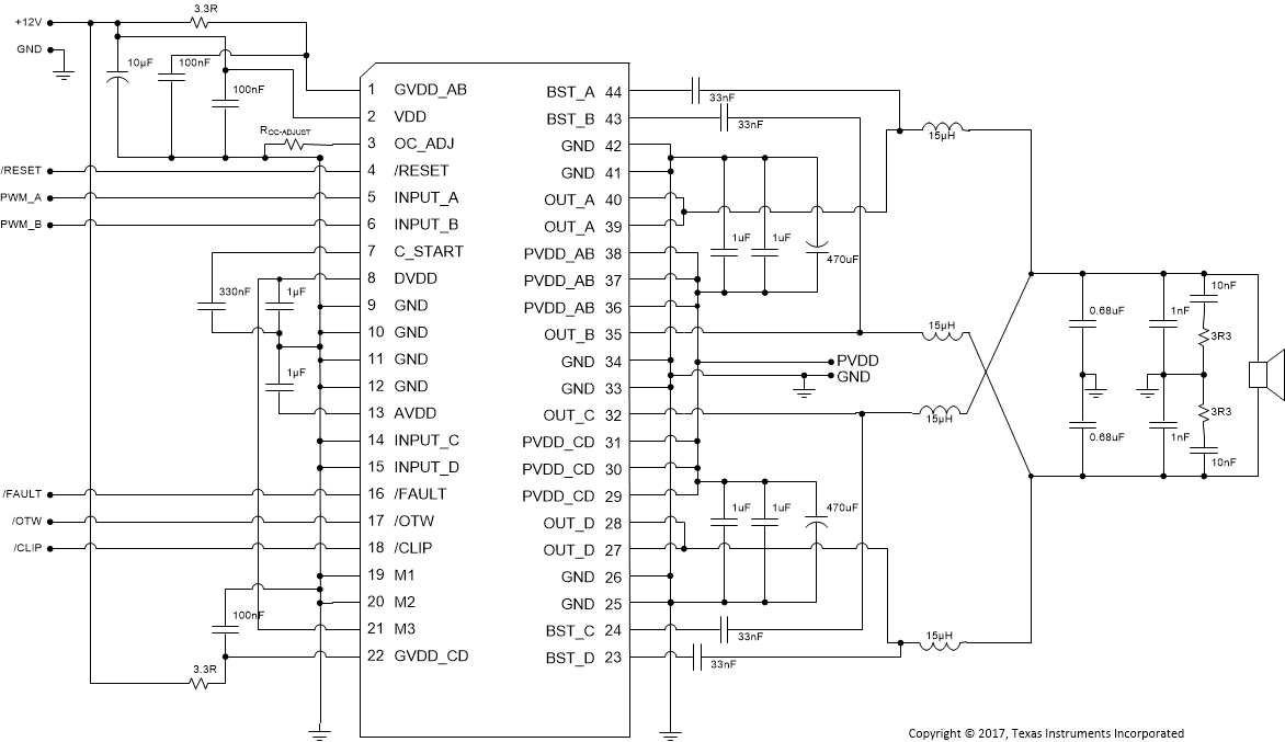
These typical connection diagrams highlight the required external components and system level connections for proper operation of the device in several common use cases. Each of these configurations can be tested using the TAS5634EVM. Please contact TI through TI.com or by visiting the TI E2E Forum at www.e2e.ti.com for design assistance and join the audio amplifier discussion forum for additional information.
9.2 Typical Applications
9.2.1 Typical BTL Application
See Figure 26 for application schematic. In this application, differential PWM inputs are used with AD modulation from the PWM modulator (TAS5558). AD modulation scheme is defined as PWM(+) as opposite polarity from PWM(–).
 Figure 26. Typical Differential (2N) BTL Application
9.2.1.1 Design Requirements
For this design example, us the values shown in Table 7.
Table 7. BTL Design Requirements
| PARAMETERS | VALUES |
|---|---|
| PVDD Supply Voltage | 12 V to 58 V |
| GVDD and VDD Voltage | 12 V |
| Device Configuration | AD Modulation, Differential Input |
| Mode Pins | M3 = GND, M2 = GND, M1 = GND |
| INPUT_A | PWM_1+ |
| INPUT_B | PWM_1- |
| INPUT_C | PWM_2+ |
| INPUT_D | PWM_2- |
| PWM modulator | TAS5548 |
| Output filters | Inductor: 15 μH, Capacitor: 0.68 μF |
| Speaker | 6 Ω minimum |
| C_START Capacitor | 330 nF |
| OC_ADJ Resistor | 27 kΩ (14 A per channel, Cycle-by-cycle Current Limit) |
9.2.1.2 Detailed Design Procedure
- Follow the recommended component placement, layout and routing guidelines shown in the Layout Example section.
- The most critical section of the circuit is the power supply pins, the amplifier output signals and the high frequency signals.
- For specific application questions and support go to the TI E2E Forum at www.e2e.ti.com.
9.2.1.3 Pin Connections
- Pin 1 - GVDD_AB - The gate-drive voltage for half-bridges A and B. Place a 0.1-μF decoupling capacitor placed near the pin.
- Pin 2 - VDD - The supply pin for internal voltage regulators AVDD and DVDD. Place a 10-μF bulk capacitor and a 0.1-μF decoupling capacitor near the pin.
- Pin 3 - ROC - Programming resistor for the overcurrent (OC) threshold. Place a resistor to ground. See table OC_ADJ Resistor Value for OC Threshold for the appropriate resistor value.
- Pin 4 - RESET - Device reset. When asserted, output stage is Hi-Z and there is no PWM switching. This pin can be controlled by a switch, microcontroller or processor.
- Pins 5 and 6 - INPUT_A and INPUT_B - Differential PWM input pair for A and B BTL channel with signals provided by a PWM modulator such as the TAS5548.
- Pin 7 - C_START - Start-up ramp capacitor must be 330nf for BTL/PBTL or 1 μF for SE configuration.
- Pin 8 - DVDD - Digital output supply pin is connected to 1-μF decoupling capacitor
- Pins 9-12 - GND - Connect to board GND.
- Pin 13 - AVDD - Analog output supply pin. Connect a 1-μF decoupling capacitor to device GND, pins 9-12.
- Pins 14 and 15 - INPUT_C and INPUT_D - Differential PWM input pair for C and D BTL channel with signals provided by a PWM modulator such as the TAS5548.
- Pin 16 - FAULT - Fault pin can be monitored by a microcontroller through GPIO pin. System can decide to assert reset or shutdown.
- Pin 17 - OTW - Overtemperature warning pin can be monitored by a microcontroller through a GPIO pin. System can decide to turn on fan or lower output power.
- Pin 18 - CLIP - Output clip indicator can be monitored by a microcontroller through a GPIO pin. System can decide to lower the volume.
- Pins 19-21 - M1, M2, M3 - Mode pins set the input and output configurations. For this configuration M1-M3 are grounded. These mode pins must be hardware configured and set before starting device. Do not adjust while TAS5634 is operating.
- Pin 22 - GVDD_CD - The gate-drive voltage for half-bridges C and D. Place a 0.1-μF decoupling capacitor placed near the pin.
- Pins 23, 24, 43, 44 - BST_A, BST_B, BST_C, BST_D - Bootstrap pins for half-bridges A, B, C, and D. Connect 33 nF from this pin to corresponding output pins.
- Pins 25, 26, 33, 34, 41, 42 - GND - Connect to board ground and decoupling capacitors connected to PVDD_X.
- Pins 27, 28, 32, 35, 39, 40 - OUT_A, OUT_B, OUT_C, OUT_D - Output pins from half-bridges A, B, C, and D. Connect bootstrap capacitors and differential LC filter.
- Pins 29, 30, 31, 36, 37, 38 - PVDD_AB, PVDD_CD - Power supply pins to half-bridges A, B, C, and D. A and B form a full-bridge and C and D form another full-bridge. A 470-μF bulk capacitor is recommended for each full-bridge power pins. Place one 1-μF decoupling capacitor next to each pin.
9.2.1.4 Application Curves


9.2.2 Typical PBTL Configuration
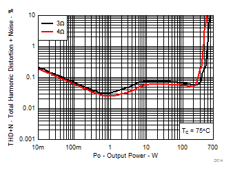
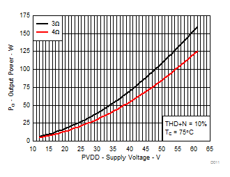
Use the sectionDetailed Design Procedure in the Typical BTL Application section for a pin description and setup.
 Figure 29. Typical Differential (2N) PBTL Application
Table 8. PBTL Design Requirements
| PARAMETERS | VALUES |
|---|---|
| PVDD Supply Voltage | 12 V to 58 V |
| GVDD and VDD Voltage | 12 V |
| Device Configuration | AD Modulation, Differential Input |
| Mode Pins | M3 = DVDD, M2 = GND, M1 = GND |
| INPUT_A | PWM_A+ |
| INPUT_B | PWM_A- |
| INPUT_C | GND |
| INPUT_D | GND |
| PWM modulator | TAS5548 |
| Output filters | Inductor: 15 μH, Capacitor: 0.68 μF |
| Speaker | 3 Ω minimum |
| C_START Capacitor | 330 nF |
| OC_ADJ Resistor | 27 kΩ (14 A per channel, Cycle-by-cycle Current Limit) |
9.2.2.1 Application Curves


9.2.3 Typical SE Configuration
See Figure 32 for application schematic. In this application, four single-ended PWM inputs are used with AD modulation from the PWM modulator such as the TAS5558. AD modulation scheme is defined as PWM(+) is opposite polarity from PWM(–), but in this case there is only a single-ended signal. The single-ended (SE) output configuration is often used to drive four independent channels in one TAS5634 device.
 Figure 32. Typical (1N) SE Application
Table 9. SE Design Requirements
| PARAMETERS | VALUES |
|---|---|
| PVDD Supply Voltage | 12 V to 58 V |
| GVDD and VDD Voltage | 12 V |
| Device Configuration | AD Modulation, Single-Ended Input |
| Mode Pins | M3 = DVDD, M2 = GND, M1 = DVDD |
| INPUT_A | PWM_1 |
| INPUT_B | PWM_2 |
| INPUT_C | PWM_3 |
| INPUT_D | PWM_4 |
| PWM modulator | TAS5548 |
| Output filters | Inductor: 15 μH, Capacitor: 0.68 μF |
| Speaker | 3 Ω minimum |
| C_START Capacitor | 1 μF |
| OC_ADJ Resistor | 27 kΩ (14 A per channel, Cycle-by-cycle Current Limit) |
9.2.3.1 Application Curves

