SLOS836E May 2013 – June 2016 TAS5729MD
PRODUCTION DATA.
- 1 Features
- 2 Applications
- 3 Description
- 4 Revision History
- 5 Related Devices
- 6 Pin Configuration and Functions
-
7 Specifications
- 7.1 Absolute Maximum Ratings
- 7.2 ESD Ratings
- 7.3 Recommended Operating Conditions
- 7.4 Thermal Information
- 7.5 Digital I/O Pins
- 7.6 Master Clock
- 7.7 Serial Audio Port
- 7.8 Protection Circuitry
- 7.9 Speaker Amplifier in All Modes
- 7.10 Speaker Amplifier in Stereo Bridge Tied Load (BTL) Mode
- 7.11 Speaker Amplifier in Stereo Post-Filter Parallel Bridge Tied Load (Post-Filter PBTL) Mode
- 7.12 Headphone Amplifier and Line Driver
- 7.13 Reset Timing
- 7.14 I2C Control Port
- 7.15 Typical Electrical Power Consumption
- 7.16 Typical Characteristics
- 8 Parameter Measurement Information
-
9 Detailed Description
- 9.1 Overview
- 9.2 Functional Block Diagram
- 9.3 Feature Description
- 9.4 Device Functional Modes
- 9.5 Programming
- 9.6
Register Maps
- 9.6.1 Clock Control Register (0x00)
- 9.6.2 Device ID Register (0x01)
- 9.6.3 Error Status Register (0x02)
- 9.6.4 System Control Register 1 (0x03)
- 9.6.5 Serial Data Interface Register (0x04)
- 9.6.6 System Control Register 2 (0x05)
- 9.6.7 Soft Mute Register (0x06)
- 9.6.8 Volume Registers (0x07, 0x08, 0x09)
- 9.6.9 Volume Configuration Register (0x0E)
- 9.6.10 Modulation Limit Register (0x10)
- 9.6.11 Interchannel Delay Registers (0x11, 0x12, 0x13, and 0x14)
- 9.6.12 PWM Shutdown Group Register (0x19)
- 9.6.13 Start/Stop Period Register (0x1A)
- 9.6.14 Oscillator Trim Register (0x1B)
- 9.6.15 BKND_ERR Register (0x1C)
- 9.6.16 Input Multiplexer Register (0x20)
- 9.6.17 Channel 4 Source Select Register (0x21)
- 9.6.18 PWM Output MUX Register (0x25)
- 9.6.19 AGL Control Register (0x46)
- 9.6.20 PWM Switching Rate Control Register (0x4F)
- 9.6.21 EQ Control (0x50)
-
10Application and Implementation
- 10.1 Application Information
- 10.2
Typical Applications
- 10.2.1 Stereo BTL Configuration With Headphone and Line Driver Amplifier
- 10.2.2 Mono PBTL Configuration with Headphone and Line Driver Amplifier
- 11Power Supply Recommendations
- 12Layout
- 13Device and Documentation Support
- 14Mechanical, Packaging, and Orderable Information
パッケージ・オプション
メカニカル・データ(パッケージ|ピン)
- DCA|48
サーマルパッド・メカニカル・データ
- DCA|48
発注情報
9 Detailed Description
9.1 Overview
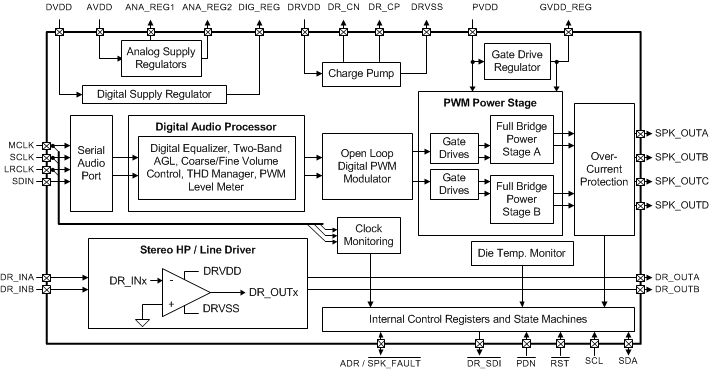
The TAS5729MD is a stereo I2S input Class-D amplifier with a digital audio processor and a DirectPath™ headphone/line driver.
Digital auto processor features two-band advanced automatic gain limiting (AGL), digital equalization, course and fine volume control, and PWM Level meter. The AGL is an enhanced dynamic range compression (DRC) function.
The device requires only a single DVDD supply in addition to the higher-voltage PVDD power supply. The wide PVDD power supply range of the device enables its use in a multitude of applications.
The TAS5729MD is a slave-only device that is controlled by a bidirectional I2C interface that supports both 100-kHz and 400-kHz data transfer rates for single- and multiple-byte write and read operations. This control interface is used to program the registers of the device and read the device status.
The device has an integrated DirectPath headphone amplifier / line driver to increase system level integration and reduce total solution costs. DirectPath architecture eliminates the requirement for external dc-blocking output capacitors.
An optimal mix of thermal performance and device cost is provided in the 200-mΩ RDS(ON) of the output MOSFETs. Additionally, a thermally enhanced 48-pin HTSSOP provides excellent operation in the elevated ambient temperatures found in modern consumer electronic devices.
9.2 Functional Block Diagram
9.3 Feature Description
9.3.1 Power Supply
To facilitate system design, the TAS5729MD requires only a single low-voltage DVDD supply in addition to the higher-voltage PVDD power supply. An internal voltage regulator provides suitable voltage levels for the gate drive circuitry. Additionally, all circuitry requiring a floating voltage supply (for example, the high-side gate drive) is accommodated by built-in bootstrap circuitry requiring only a few external capacitors.
To provide good electrical and acoustical characteristics, the PWM signal path for the output stage is designed as identical, independent half-bridges that operate in pairs to produce the full-bridge outputs capable of driving BTL loads. For this reason, each half-bridge has separate bootstrap pins (BSTRPx) and power-stage supply pins (PVDD). The gate drive voltage (GVDD_REG) is derived from the PVDD voltage. Special attention should be paid to placing all decoupling capacitors as close to their associated pins as possible. In general, inductance between the power-supply pins and decoupling capacitors must be avoided.
For a properly functioning bootstrap circuit, a small ceramic capacitor must be connected from each bootstrap pin (BSTRPx) to the power-stage output pin (SPK_OUTx). When the power-stage output is low, the bootstrap capacitor is charged through an internal diode connected between the gate-drive regulator output pin (GVDD_REG) and the bootstrap pin. When the power-stage output is high, the bootstrap capacitor potential is shifted above the output potential and thus provides a suitable voltage supply for the high-side gate driver.
Special attention should be paid to the power-stage power supply; this includes component selection, PCB placement, and routing. As indicated, each pair of half-bridges has independent power-stage supply pins (PVDD). For optimal electrical performance, EMI compliance, and system reliability, each PVDD pin must be decoupled with a ceramic capacitor placed as close as possible to each supply pin, as shown in Typical Applications.
9.3.2 ADR/SPK_FAULT
The ADR/SPK_FAULT pin is an input pin during power-up, and can be pulled high or low through a pullup or pulldown resistor, as shown in Typical Applications. High sets an I2C address of 101011[R/W], and low sets an address of 101010[R/W]. Additionally, via the control port, the ADR/SPK_FAULT pin can be configured to serve as the fault indicator for the speaker amplifier.
9.3.3 Device Protection System
9.3.3.1 Overcurrent (OC) Protection With Current Limiting
The device has independent, fast-reacting current detectors on all high-side and low-side power-stage FETs. The detector outputs are closely monitored by a protection system. If a high-current condition persists, that is, the power stage is being overloaded, a protection system triggers a shutdown resulting in the power stage being set in the high-impedance (Hi-Z) state. The device retries to start-up based on the retry time set in the BKDN_ERR register and returns to normal operation once the fault condition (that is, a short-circuit on the output) is removed. Current limiting and overcurrent protection are not independent for half-bridges. That is, if the bridge-tied load between half-bridges A and B causes an overcurrent fault, half-bridges A, B, C, and D are shutdown. An overcurrent fault error is reported in the ERROR STATUS register, and a fault error signal can be monitored on the SPK_FAULT pin if configured in the system control register.
9.3.3.2 Overtemperature Protection
The TAS5729MD has an overtemperature-protection system. If the device junction temperature exceeds the amount specified by OTETHRES in the Protection Circuitry table, the device is put into thermal shutdown, resulting in all half-bridge outputs being set in the high-impedance (Hi-Z) state. The TAS5729MD recovers automatically once the temperature drops by the amount specified by OTEHYST. An overtemperature fault error is reported in the ERROR STATUS register, and a fault error signal can be monitored on the SPK_FAULT pin if configured in the system control register.
9.3.3.3 Undervoltage Error (UVE) and Power-On Reset (POR)
The UVE and POR circuits of the TAS5729MD fully protect the device in any power-up, powerdown, or brownout situation. While powering up, the POR circuit ensures that all circuits are fully operational when the PVDD and AVDD supply voltages reach their respective UVETHRES levels as specified in the Protection Circuitry table. Although PVDD and AVDD are independently monitored, a supply voltage drop below the UVE threshold for AVDD or either of the PVDD pins results in all half-bridge outputs immediately being set in the high-impedance (Hi-Z) state. An undervoltage fault error is reported in the ERROR STATUS register, and a fault error signal can be monitored on the SPK_FAULT pin if configured in the system control register.
9.3.4 Clock, Auto Detection, and PLL
The TAS5729MD is an I2S slave device that requires a valid master clock (MCLK), bit clock (SCLK), and word clock (LRCLK) to play audio. The digital audio processor (DAP) supports all of the sample rates and MCLK rates that are defined in the Clock Control Register (0x00). The TAS5729MD checks to verify that SCLK is a specific value of 32 × fS, 48 × fS, or 64 × fS. The DAP only supports a 1 × fS LRCLK.
The device has robust clock error handling that uses a built-in auto detect block to quickly detect changes or errors. When the system detects a clock change or error, it mutes the audio (through a single-step mute) and forces PLL to limp, where output PWMs continue to switch in idle but the device cannot play audio. Once the clocks are valid and stable, the system auto detects the new rate and reverts to normal operation. During this process, the volume is restored in a single step (also called hard unmute). The ramp process can be programmed to ramp back slowly (also called soft unmute) as defined in volume register (0x0E).
Table 1 shows the valid MCLK rates across different fS rates. For 44.1-kHz or 48-kHz fS rates, a 64 × fS MCLK rate is supported. If a 64 × fS SCLK rate is used, a common 64 × fS clock can be used for both MCLK and SCLK.
Table 1. Supported LRCLK, SCLK, and MCLK Ratios in the TAS5729MD
| LRCLK Rate [kHz] |
MCLK Rate [ × fS] | |||||
|---|---|---|---|---|---|---|
| 64 | 128 | 192 | 256 | 384 | 512 | |
| 8 | — | — | — | — | Y | Y |
| 11.025 or 12 | — | — | — | Y | Y | Y |
| 16 | — | — | — | Y | Y | Y |
| 22.05 or 24 | — | — | — | Y | Y | Y |
| 32 | — | — | Y | Y | Y | Y |
| 44.1 or 48 | Y | Y | Y | Y | Y | Y |
9.3.5 Serial Data Interface
Serial data is input on SDIN. The PWM outputs are derived from SDIN. The TAS5729MD DAP accepts serial data in 16-, 20-, or 24-bit left-justified, right-justified, or I2S serial data format.
9.3.6 PWM Section
The TAS5729MD DAP device uses noise-shaping and sophisticated nonlinear correction algorithms to achieve high-power efficiency and high-performance digital audio reproduction. The DAP uses a fourth-order noise shaper to increase dynamic range and SNR in the audio band. The PWM section accepts 24-bit PCM data from the DAP and outputs two BTL PWM audio output channels.
The PWM section has internal dc-blocking filters that can be enabled and disabled using the System Control Register 1 (0x03). The controls for the dc-blocking filters are ganged together and enabling or disabling will affect both channels simultaneously. The filter cutoff frequency is less than 1 Hz. Individual-channel de-emphasis filters for 44.1 kHz and 48 kHz are included and can be enabled and disabled.
Finally, the PWM section has an adjustable maximum modulation limit of 93.8% to 99.2%.
9.3.7 I2C Compatible Serial Control Interface
The TAS5729MD DAP has an I2C serial control slave interface to receive commands from a system controller. The serial control interface supports both normal-speed (100 kHz) and high-speed (400 kHz) operations without wait states. As an added feature, this interface operates even if MCLK is absent.
The serial control interface supports both single-byte and multiple-byte read and write operations for status registers and the general control registers associated with the PWM.
9.3.8 Serial Interface Control And Timing
9.3.8.1 I2S Timing
I2S timing uses LRCLK to define when the data being transmitted is for the left channel and when the data is for the right channel. LRCLK is low for the left channel and high for the right channel. A bit clock running at 32, 48, or 64 × fS is used to clock in the data. A delay of one bit clock exists from the time the LRCLK signal changes state to the first bit of data on the data lines. The data is written MSB-first and is valid on the rising edge of bit clock. The DAP masks unused trailing data-bit positions.
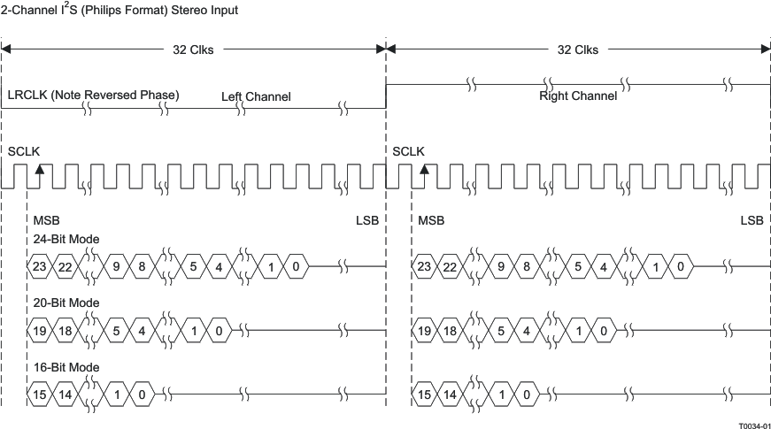
NOTE:
All data presented in 2s-complement form with MSB first.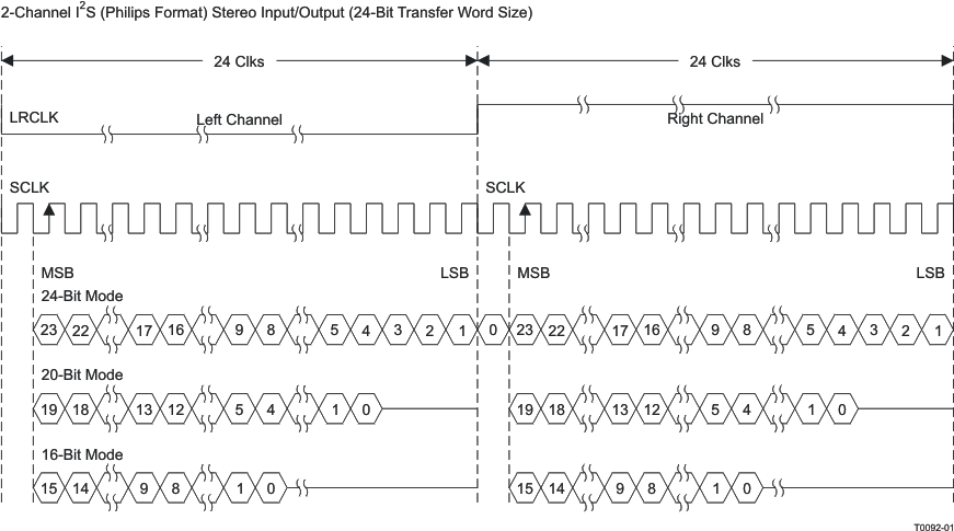
NOTE:
All data presented in 2s-complement form with MSB first.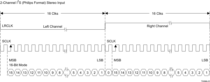
NOTE:
All data presented in 2s-complement form with MSB first.9.3.8.2 Left-Justified
Left-justified (LJ) timing uses LRCLK to define when the data being transmitted is for the left channel and when the data is for the right channel. LRCLK is high for the left channel and low for the right channel. A bit clock running at 32, 48, or 64 × fS is used to clock in the data. The first bit of data appears on the data lines at the same time LRCLK toggles. The data is written MSB-first and is valid on the rising edge of the bit clock. The DAP masks unused trailing data-bit positions.
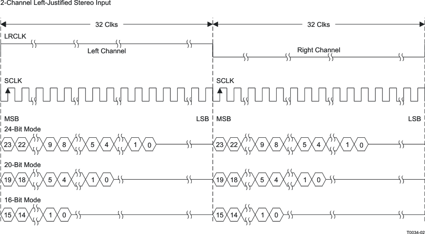
NOTE:
All data presented in 2s-complement form with MSB first.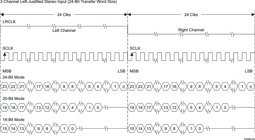
NOTE:
All data presented in 2s-complement form with MSB first.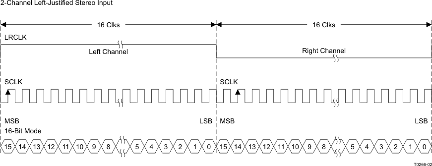
NOTE:
All data presented in 2s-complement form with MSB first.9.3.8.3 Right-Justified
Right-justified (RJ) timing uses LRCLK to define when the data being transmitted is for the left channel and when the data is for the right channel. LRCLK is high for the left channel and low for the right channel. A bit clock running at 32, 48, or 64 × fS is used to clock in the data. The first bit of data appears on the data 8 bit-clock periods (for 24-bit data) after LRCLK toggles. In RJ mode the LSB of data is always clocked by the last bit clock before LRCLK transitions. The data is written MSB-first and is valid on the rising edge of bit clock. The DAP masks unused leading data-bit positions.
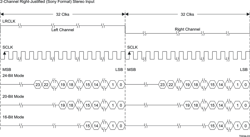 Figure 38. Right-Justified 64 × fS Format
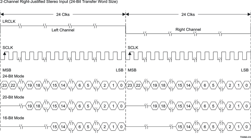 Figure 39. Right-Justified 48 × fS Format
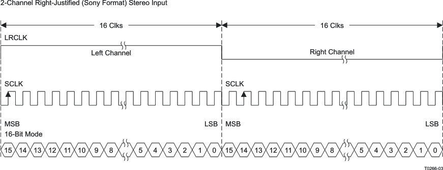 Figure 40. Right-Justified 32 × fS Format
9.3.9 Automatic Gain Limiting (AGL)
The AGL scheme has two AGL blocks. The high-band left/right channels have one ganged AGL and the low-band left/right channels have the other AGL.
The AGL input/output diagram is shown in Figure 41.
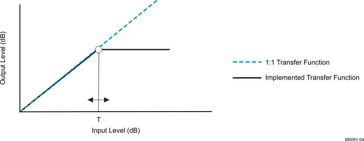
• Each AGL has adjustable threshold levels.
• Programmable attack and release rate
• Transparent compression: compressors can attack fast enough to avoid apparent clipping before engaging,
and decay times can be set slow enough to avoid pumping.
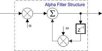
| α, ω | T | αa, ωa / αd, φd | |
|---|---|---|---|
| AGL1 | 0x3B | 0x40 | 0x3C |
| AGL2 | 0x3E | 0x43 | 0x3F |
9.3.10 PWM Level Meter
The structure in Figure 43 shows the PWM level meter that can be used to study the power profile.
 Figure 43. PWM Level Meter Structure
9.4 Device Functional Modes
9.4.1 Device Protection Mode
The TAS5729MD contains a complete set of protection circuits carefully designed to make system design efficient as well as to protect the device against any kind of permanent failures due to overcurrent, overtemperature, and undervoltage. Any of these errors are reported in the ERROR STATUS register, and a fault error signal can be monitored on the SPK_FAULT pin if configured in the system control register. If any of the protection circuits is activated, all half-bridge outputs are immediately set in the high-impedance (hi-Z) state.
9.4.2 Speaker Amplifier Mode
The TAS5729MD can be configured in different amplifier configurations:
- Stereo BTL mode
- Monaural PBTL mode
9.4.2.1 Stereo Mode
The classic stereo mode of operation uses the TAS5729MD device to amplify two independent signals that represent the left and right portions of a stereo signal. These amplified left and right audio signals are presented on differential output pairs shown as SPK_OUTA and SPK_OUTB for channel 1 and SPK_OUTC and SPK_OUTD for channel 2. The routing of the audio data that is presented on the SPK_OUTx outputs can be changed according to the PWM Output Mux Register (0x25). By default, the TAS5729MD device is configured to output channel 1 to the SPK_OUTA and SPK_OUTB outputs, and channel 2 to the SPK_OUTC and SPK_OUTD outputs. Stereo mode operation outputs are shown in Figure 44.
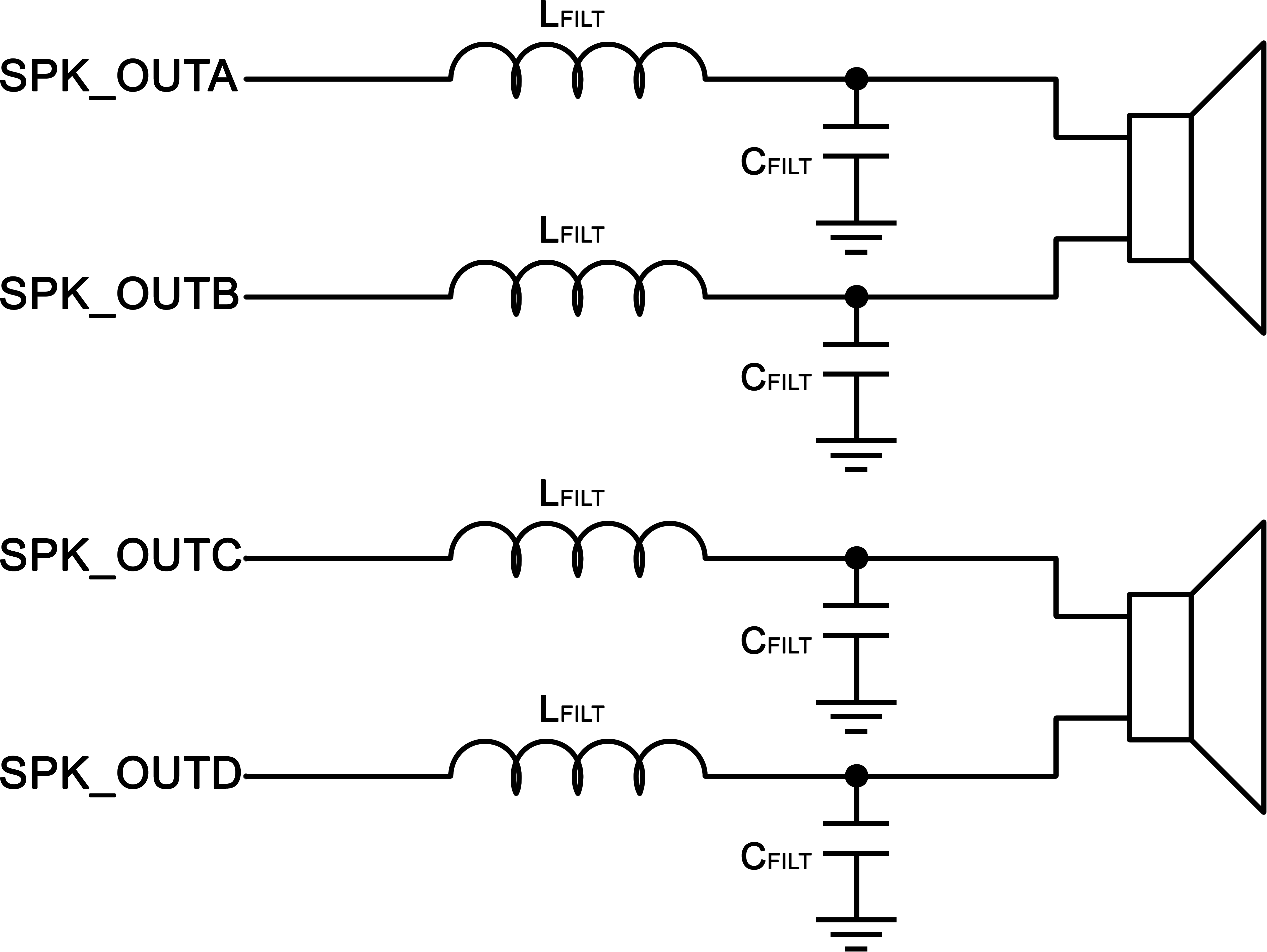 Figure 44. Stereo BTL Mode
9.4.2.2 Monaural Mode
When this mode of operation is used, the two stereo outputs of the device are placed in parallel, one with another to increase the power sourcing capabilities of the device. On the output side of the TAS5729MD device, the merging of the two output channels is done after the inductor portion of the output filter. Doing so requires two additional inductors, but allows smaller, less expensive inductors to be used because the current is divided between the two inductors. This process is called post-filter PBTL, and the monaural operation is shown in Figure 45.
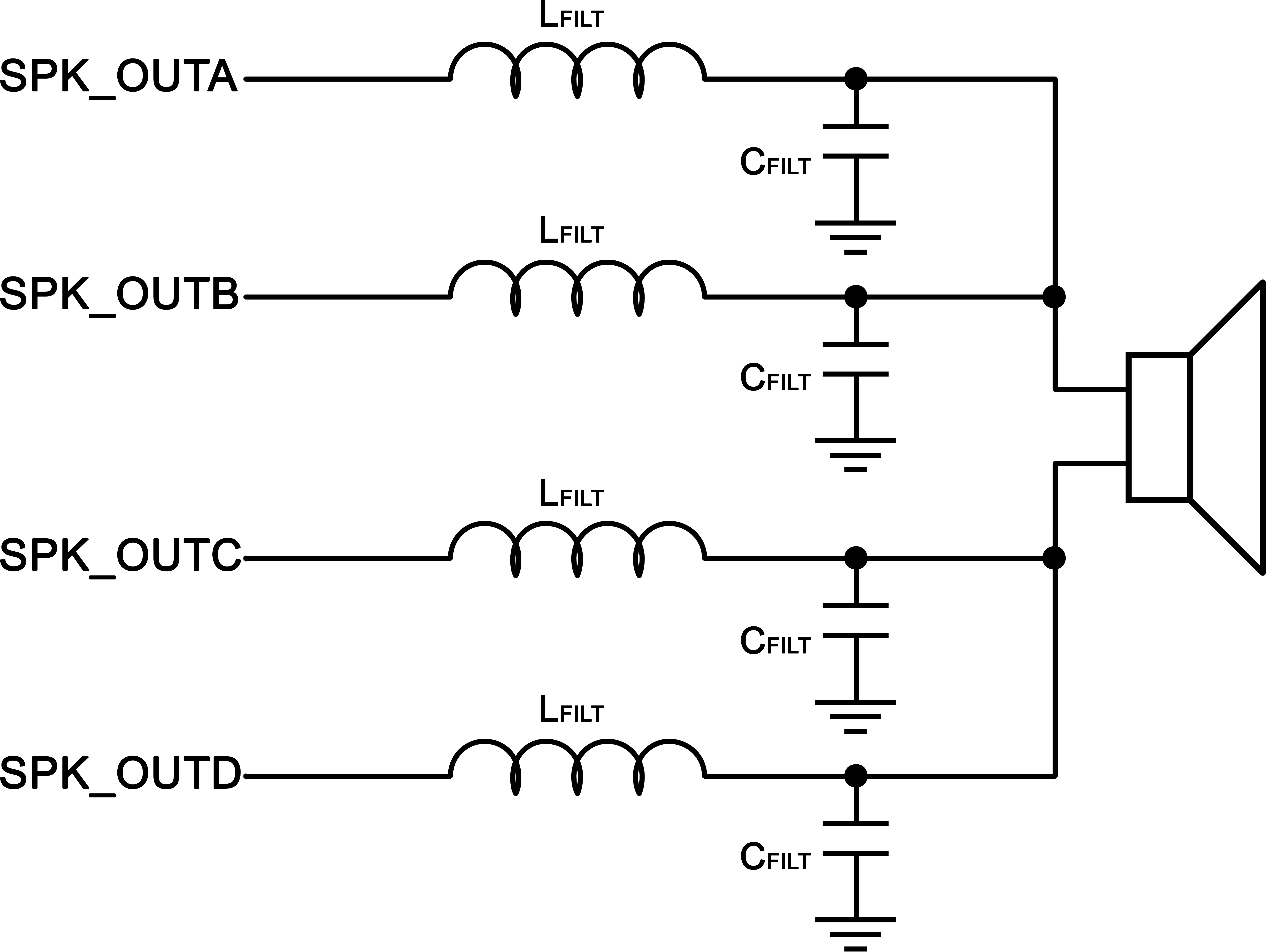 Figure 45. Post-Filter PBTL
On the input side of the TAS5729MD device, the input signal to the monaural amplifier can be selected from a mix, left, or right frame from an I2S, LJ, or RJ signal. The routing of the audio data which is presented on the SPK_OUTx outputs must be configured with the PWM Output Mux Register (0x25).
9.4.3 Headphone/Line Amplifier
An integrated ground centered DirectPath combination headphone amplifier and line driver is integrated in the TAS5729MD. This headphone/line amplifier can be used independently from the device speaker amplifier modes, with analog single-ended inputs DR_INA and DR_INB, linked to the respective analog outputs DR_OUTA, and DR_OUTB. A basic diagram of the headphone/line amplifier is shown in Figure 46.
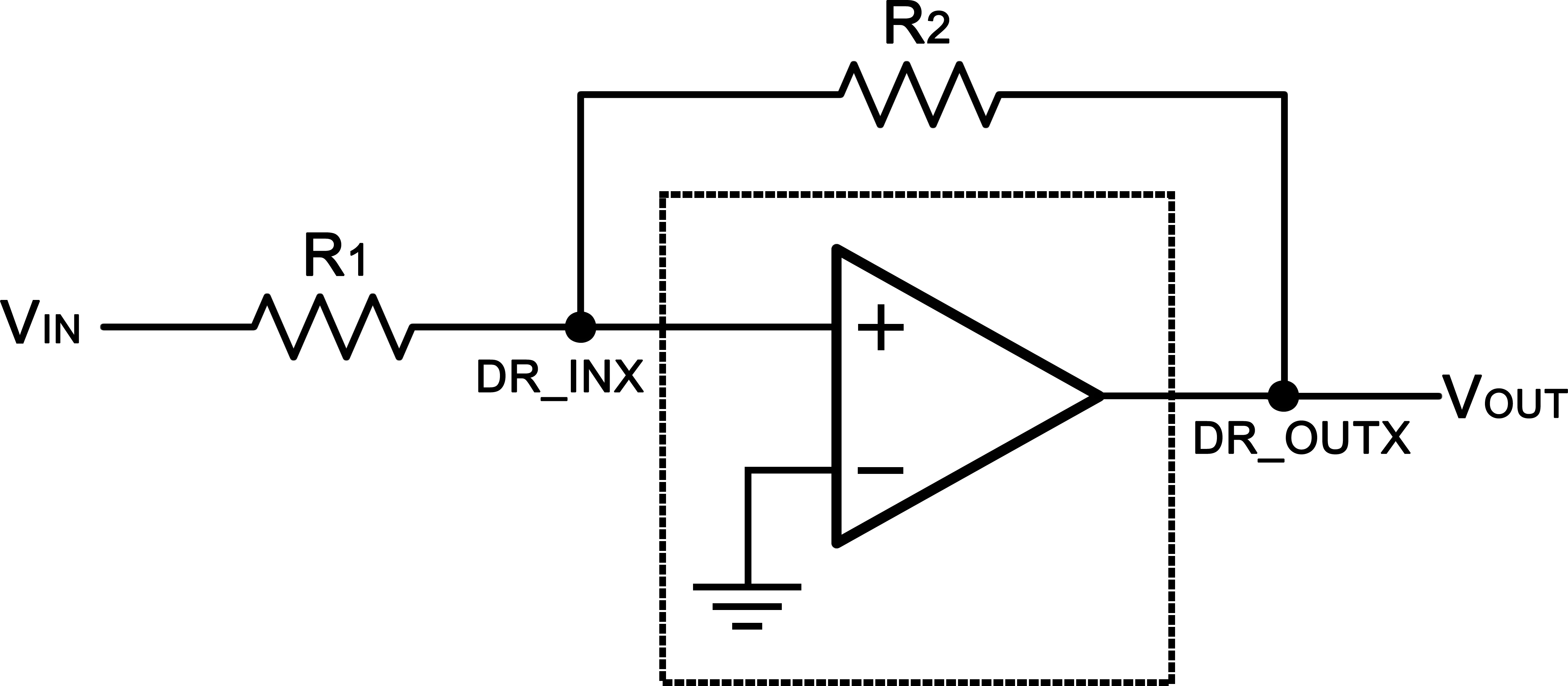 Figure 46. Headphone/Line Amplifier
The DR_SDI pin can be used to turn on or off the headphone amplifier and line driver. The DirectPath amplifier makes use of the provided positive and negative supply rails generated by the IC. The output voltages are centered at zero volts with the capability to swing to the positive rail or negative rail; combining this capability with the built-in click and pop reduction circuit, the DirectPath amplifier requires no output dc blocking capacitors.
9.5 Programming
9.5.1 I2C Serial Control Interface
The TAS5729MD DAP has a bidirectional I2C interface that is compatible with the I2C bus protocol and supports both 100-kHz and 400-kHz data transfer rates for single- and multiple-byte write and read operations. The DAP is a slave-only device that does not support a multimaster bus environment or wait-state insertion. The control interface is used to program the registers of the device and to read device status.
The DAP supports the standard-mode I2C bus operation (100 kHz maximum) and the fast I2C bus operation (400 kHz maximum). The DAP performs all I2C operations without I2C wait cycles.
9.5.1.1 General I2C Operation
The I2C bus employs two signals: SDA (data) and SCL (clock), to communicate between integrated circuits in a system. Data is transferred on the bus serially, one bit at a time. The address and data can be transferred in byte (8-bit) format, with the most significant bit (MSB) transferred first. In addition, each byte transferred on the bus is acknowledged by the receiving device with an acknowledge bit.
Each transfer operation begins with the master device driving a start condition on the bus and ends with the master device driving a stop condition on the bus. The bus uses transitions on the data pin (SDA) while the clock is high to indicate start and stop conditions. A high-to-low transition on SDA indicates a start and a low-to-high transition indicates a stop. Normal data-bit transitions must occur within the low time of the clock period. These conditions are shown in Figure 47.
The master generates the 7-bit slave address and the read/write (R/W) bit to open communication with another device and then waits for an acknowledge condition. The TAS5729MD holds SDA low during the acknowledge clock period to indicate an acknowledgment. When this occurs, the master transmits the next byte of the sequence. Each device is addressed by a unique 7-bit slave address plus R/W bit (1 byte). All compatible devices share the same signals via a bidirectional bus using a wired-AND connection. An external pullup resistor must be used for the SDA and SCL signals to set the high level for the bus.
 Figure 47. Typical I2C Sequence
An unlimited number of bytes can be transmitted between start and stop conditions. When the last word transfers, the master generates a stop condition to release the bus. A generic data transfer sequence is shown in Figure 47.
9.5.1.2 Single- and Multiple-Byte Transfers
The serial control interface supports both single-byte and multiple-byte read/write operations for subaddresses 0x00 to 0x1F. However, for the subaddresses 0x20 to 0xFF, the serial control interface supports only multiple-byte read/write operations (in multiples of 4 bytes).
During multiple-byte read operations, the DAP responds with data, a byte at a time starting at the subaddress assigned, as long as the master device continues to respond with acknowledges. If a particular subaddress does not contain 32 bits, the unused bits are read as logic 0.
During multiple-byte write operations, the DAP compares the number of bytes transmitted to the number of bytes that are required for each specific subaddress. For example, if a write command is received for a biquad subaddress, the DAP expects to receive five 32-bit words. If fewer than five 32-bit data words have been received when a stop command (or another start command) is received, the data received is discarded.
Supplying a subaddress for each subaddress transaction is referred to as random I2C addressing. The TAS5729MD also supports sequential I2C addressing. For write transactions, if a subaddress is issued followed by data for that subaddress and the 15 subaddresses that follow, a sequential I2C write transaction has taken place, and the data for all 16 subaddresses is successfully received by the TAS5729MD. For I2C sequential write transactions, the subaddress then serves as the start address, and the amount of data subsequently transmitted, before a stop or start is transmitted, determines how many subaddresses are written. As was true for random addressing, sequential addressing requires that a complete set of data be transmitted. If only a partial set of data is written to the last subaddress, the data for the last subaddress is discarded. However, all other data written is accepted; only the incomplete data is discarded.
9.5.1.3 Single-Byte Write
As shown in Figure 48, a single-byte data-write transfer begins with the master device transmitting a start condition followed by the I2C device address and the read/write bit. The read/write bit determines the direction of the data transfer. For a data-write transfer, the read/write bit is 0. After receiving the correct I2C device address and the read/write bit, the DAP responds with an acknowledge bit. Next, the master transmits the address byte or bytes corresponding to the TAS5729MD internal memory address being accessed. After receiving the address byte, the TAS5729MD again responds with an acknowledge bit. Next, the master device transmits the data byte to be written to the memory address being accessed. After receiving the data byte, the TAS5729MD again responds with an acknowledge bit. Finally, the master device transmits a stop condition to complete the single-byte data-write transfer.
 Figure 48. Single-Byte Write Transfer
9.5.1.4 Multiple-Byte Write
A multiple-byte data-write transfer is identical to a single-byte data write transfer except that multiple data bytes are transmitted by the master device to the DAP as shown in Figure 49. After receiving each data byte, the TAS5729MD responds with an acknowledge bit.
 Figure 49. Multiple-Byte Write Transfer
9.5.1.5 Single-Byte Read
As shown in Figure 50, a single-byte data-read transfer begins with the master device transmitting a start condition followed by the I2C device address and the read/write bit. For the data-read transfer, both a write followed by a read are actually done. Initially, a write is done to transfer the address byte or bytes of the internal memory address to be read. As a result, the read/write bit becomes a 0. After receiving the TAS5729MD address and the read/write bit, TAS5729MD responds with an acknowledge bit. In addition, after sending the internal memory address byte or bytes, the master device transmits another start condition followed by the TAS5729MD address and the read/write bit again. This time the read/write bit becomes a 1, indicating a read transfer. After receiving the address and the read/write bit, the TAS5729MD again responds with an acknowledge bit. Next, the TAS5729MD transmits the data byte from the memory address being read. After receiving the data byte, the master device transmits a not-acknowledge followed by a stop condition to complete the single-byte data-read transfer.
 Figure 50. Single-Byte Read Transfer
9.5.1.6 Multiple-Byte Read
A multiple-byte data-read transfer is identical to a single-byte data-read transfer except that multiple data bytes are transmitted by the TAS5729MD to the master device as shown in Figure 51. Except for the last data byte, the master device responds with an acknowledge bit after receiving each data byte.
 Figure 51. Multiple-Byte Read Transfer
9.5.2 26-Bit 3.23 Number Format
All mixer gain coefficients are 26-bit coefficients using a 3.23 number format. A number formatted as a 3.23 number means that the binary point has three bits to the left and 23 bits to the right. This configuration is shown in Figure 52.
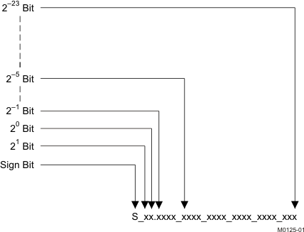 Figure 52. 3.23 Format
The decimal value of a 3.23 format number can be found by following the weighting shown in Figure 52. If the most significant bit is logic 0, the number is a positive number, and the weighting shown yields the correct number. If the most significant bit is a logic 1, then the number is a negative number. In this case every bit must be inverted, a 1 added to the result, and then the weighting shown in Figure 53 applied to obtain the magnitude of the negative number.
 Figure 53. Conversion Weighting Factors—3.23 Format to Floating Point
Gain coefficients, entered via the I2C bus, must be entered as 32-bit binary numbers. The format of the 32-bit number (4-byte or 8-digit hexadecimal number) is shown in Figure 54.
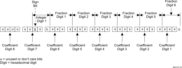 Figure 54. Alignment of 3.23 Coefficient in 32-Bit I2C Word
Table 2. Sample Calculation for 3.23 Format
| dB | LINEAR | DECIMAL | HEX (3.23 FORMAT) |
|---|---|---|---|
| 0 | 1 | 8,388,608 | 80 0000 |
| 5 | 1.77 | 14,917,288 | 00E3 9EA8 |
| –5 | 0.56 | 4,717,260 | 0047 FACC |
| X | L = 10(X/20) | D = 8388608 × L | H = dec2hex (D, 8) |
Table 3. Sample Calculation for 9.17 Format
| dB | LINEAR | DECIMAL | HEX (9.17 FORMAT) |
|---|---|---|---|
| 0 | 1 | 131,072 | 20 000 |
| 5 | 1.77 | 231,997 | 38 A3D |
| –5 | 0.56 | 73,400 | 11 EB8 |
| X | L = 10(X/20) | D = 131,072 × L | H = dec2hex (D, 8) |
9.6 Register Maps
Table 4. Serial Control Interface Register Summary
| SUBADDRESS | REGISTER NAME | NO. OF BYTES | CONTENTS | DEFAULT VALUE |
|---|---|---|---|---|
| A u indicates unused bits. | ||||
| 0x00 | Clock control register | 1 | Description shown in subsequent section | 0x6C |
| 0x01 | Device ID register | 1 | Description shown in subsequent section | 0xC1 |
| 0x02 | Error status register | 1 | Description shown in subsequent section | 0x00 |
| 0x03 | System control register 1 | 1 | Description shown in subsequent section | 0xA0 |
| 0x04 | Serial data interface register | 1 | Description shown in subsequent section | 0x05 |
| 0x05 | System control register 2 | 1 | Description shown in subsequent section | 0x40 |
| 0x06 | Soft mute register | 1 | Description shown in subsequent section | 0x00 |
| 0x07 | Master volume | 2 | Description shown in subsequent section | 0x03FF (mute) |
| 0x08 | Channel 1 vol | 2 | Description shown in subsequent section | 0x00C0 (0 dB) |
| 0x09 | Channel 2 vol | 2 | Description shown in subsequent section | 0x00C0 (0 dB) |
| 0x0A | Channel 3 vol | 2 | Description shown in subsequent section | 0x00C0 (0 dB) |
| 0x0B–0x0D | 1 | Reserved(1) | ||
| 0x0E | Volume configuration register | 1 | Description shown in subsequent section | 0xF0 |
| 0x0F | 1 | Reserved(1) | ||
| 0x10 | Modulation limit register | 1 | Description shown in subsequent section | 0x01 |
| 0x11 | IC delay channel 1 | 1 | Description shown in subsequent section | 0xAC |
| 0x12 | IC delay channel 2 | 1 | Description shown in subsequent section | 0x54 |
| 0x13 | IC delay channel 3 | 1 | Description shown in subsequent section | 0xAC |
| 0x14 | IC delay channel 4 | 1 | Description shown in subsequent section | 0x54 |
| 0x15–0x18 | 1 | Reserved(1) | ||
| 0x19 | PWM Shutdown Group Register | 1 | Description shown in subsequent section | 0x30 |
| 0x1A | Start/stop period register | 1 | 0x68 | |
| 0x1B | Oscillator trim register | 1 | 0x82 | |
| 0x1C | BKND_ERR register | 1 | 0x57 | |
| 0x1D–0x1F | 1 | Reserved(1) | ||
| 0x20 | Input MUX register | 4 | Description shown in subsequent section | 0x0001 7772 |
| 0x21 | Ch 4 source select register | 4 | Description shown in subsequent section | 0x0000 4303 |
| 0x22–0x24 | 4 | Reserved(1) | ||
| 0x25 | PWM MUX register | 4 | Description shown in subsequent section | 0x0102 1345 |
| 0x26 | ch1_bq[0] | 20 | u[31:26], b0[25:0] | 0x0080 0000 |
| u[31:26], b1[25:0] | 0x0000 0000 | |||
| u[31:26], b2[25:0] | 0x0000 0000 | |||
| u[31:26], a1[25:0] | 0x0000 0000 | |||
| u[31:26], a2[25:0] | 0x0000 0000 | |||
| 0x27 | ch1_bq[1] | 20 | u[31:26], b0[25:0] | 0x0080 0000 |
| u[31:26], b1[25:0] | 0x0000 0000 | |||
| u[31:26], b2[25:0] | 0x0000 0000 | |||
| u[31:26], a1[25:0] | 0x0000 0000 | |||
| u[31:26], a2[25:0] | 0x0000 0000 | |||
| 0x28 | ch1_bq[2] | 20 | u[31:26], b0[25:0] | 0x0080 0000 |
| u[31:26], b1[25:0] | 0x0000 0000 | |||
| u[31:26], b2[25:0] | 0x0000 0000 | |||
| u[31:26], a1[25:0] | 0x0000 0000 | |||
| u[31:26], a2[25:0] | 0x0000 0000 | |||
| 0x29 | ch1_bq[3] | 20 | u[31:26], b0[25:0] | 0x0080 0000 |
| u[31:26], b1[25:0] | 0x0000 0000 | |||
| u[31:26], b2[25:0] | 0x0000 0000 | |||
| u[31:26], a1[25:0] | 0x0000 0000 | |||
| u[31:26], a2[25:0] | 0x0000 0000 | |||
| 0x2A | ch1_bq[4] | 20 | u[31:26], b0[25:0] | 0x0080 0000 |
| u[31:26], b1[25:0] | 0x0000 0000 | |||
| u[31:26], b2[25:0] | 0x0000 0000 | |||
| u[31:26], a1[25:0] | 0x0000 0000 | |||
| u[31:26], a2[25:0] | 0x0000 0000 | |||
| 0x2B | ch1_bq[5] | 20 | u[31:26], b0[25:0] | 0x0080 0000 |
| u[31:26], b1[25:0] | 0x0000 0000 | |||
| u[31:26], b2[25:0] | 0x0000 0000 | |||
| u[31:26], a1[25:0] | 0x0000 0000 | |||
| u[31:26], a2[25:0] | 0x0000 0000 | |||
| 0x2C | ch1_bq[6] | 20 | u[31:26], b0[25:0] | 0x0080 0000 |
| u[31:26], b1[25:0] | 0x0000 0000 | |||
| u[31:26], b2[25:0] | 0x0000 0000 | |||
| u[31:26], a1[25:0] | 0x0000 0000 | |||
| u[31:26], a2[25:0] | 0x0000 0000 | |||
| 0x2D | ch1_bq[7] | 20 | u[31:26], b0[25:0] | 0x0080 0000 |
| u[31:26], b1[25:0] | 0x0000 0000 | |||
| u[31:26], b2[25:0] | 0x0000 0000 | |||
| u[31:26], a1[25:0] | 0x0000 0000 | |||
| u[31:26], a2[25:0] | 0x0000 0000 | |||
| 0x2E | ch1_bq[8] | 20 | u[31:26], b0[25:0] | 0x0080 0000 |
| u[31:26], b1[25:0] | 0x0000 0000 | |||
| u[31:26], b2[25:0] | 0x0000 0000 | |||
| u[31:26], a1[25:0] | 0x0000 0000 | |||
| u[31:26], a2[25:0] | 0x0000 0000 | |||
| 0x2F | ch1_bq[9] | 20 | u[31:26], b0[25:0] | 0x0080 0000 |
| u[31:26], b1[25:0] | 0x0000 0000 | |||
| u[31:26], b2[25:0] | 0x0000 0000 | |||
| u[31:26], a1[25:0] | 0x0000 0000 | |||
| u[31:26], a2[25:0] | 0x0000 0000 | |||
| 0x30 | ch2_bq[0] | 20 | u[31:26], b0[25:0] | 0x0080 0000 |
| u[31:26], b1[25:0] | 0x0000 0000 | |||
| u[31:26], b2[25:0] | 0x0000 0000 | |||
| u[31:26], a1[25:0] | 0x0000 0000 | |||
| u[31:26], a2[25:0] | 0x0000 0000 | |||
| 0x31 | ch2_bq[1] | 20 | u[31:26], b0[25:0] | 0x0080 0000 |
| u[31:26], b1[25:0] | 0x0000 0000 | |||
| u[31:26], b2[25:0] | 0x0000 0000 | |||
| u[31:26], a1[25:0] | 0x0000 0000 | |||
| u[31:26], a2[25:0] | 0x0000 0000 | |||
| 0x32 | ch2_bq[2] | 20 | u[31:26], b0[25:0] | 0x0080 0000 |
| u[31:26], b1[25:0] | 0x0000 0000 | |||
| u[31:26], b2[25:0] | 0x0000 0000 | |||
| u[31:26], a1[25:0] | 0x0000 0000 | |||
| u[31:26], a2[25:0] | 0x0000 0000 | |||
| 0x33 | ch2_bq[3] | 20 | u[31:26], b0[25:0] | 0x0080 0000 |
| u[31:26], b1[25:0] | 0x0000 0000 | |||
| u[31:26], b2[25:0] | 0x0000 0000 | |||
| u[31:26], a1[25:0] | 0x0000 0000 | |||
| u[31:26], a2[25:0] | 0x0000 0000 | |||
| 0x34 | ch2_bq[4] | 20 | u[31:26], b0[25:0] | 0x0080 0000 |
| u[31:26], b1[25:0] | 0x0000 0000 | |||
| u[31:26], b2[25:0] | 0x0000 0000 | |||
| u[31:26], a1[25:0] | 0x0000 0000 | |||
| u[31:26], a2[25:0] | 0x0000 0000 | |||
| 0x35 | ch2_bq[5] | 20 | u[31:26], b0[25:0] | 0x0080 0000 |
| u[31:26], b1[25:0] | 0x0000 0000 | |||
| u[31:26], b2[25:0] | 0x0000 0000 | |||
| u[31:26], a1[25:0] | 0x0000 0000 | |||
| u[31:26], a2[25:0] | 0x0000 0000 | |||
| 0x36 | ch2_bq[6] | 20 | u[31:26], b0[25:0] | 0x0080 0000 |
| u[31:26], b1[25:0] | 0x0000 0000 | |||
| u[31:26], b2[25:0] | 0x0000 0000 | |||
| u[31:26], a1[25:0] | 0x0000 0000 | |||
| u[31:26], a2[25:0] | 0x0000 0000 | |||
| 0x37 | ch2_bq[7] | 20 | u[31:26], b0[25:0] | 0x0080 0000 |
| u[31:26], b1[25:0] | 0x0000 0000 | |||
| u[31:26], b2[25:0] | 0x0000 0000 | |||
| u[31:26], a1[25:0] | 0x0000 0000 | |||
| u[31:26], a2[25:0] | 0x0000 0000 | |||
| 0x38 | ch2_bq[8] | 20 | u[31:26], b0[25:0] | 0x0080 0000 |
| u[31:26], b1[25:0] | 0x0000 0000 | |||
| u[31:26], b2[25:0] | 0x0000 0000 | |||
| u[31:26], a1[25:0] | 0x0000 0000 | |||
| u[31:26], a2[25:0] | 0x0000 0000 | |||
| 0x39 | ch2_bq[9] | 20 | u[31:26], b0[25:0] | 0x0080 0000 |
| u[31:26], b1[25:0] | 0x0000 0000 | |||
| u[31:26], b2[25:0] | 0x0000 0000 | |||
| u[31:26], a1[25:0] | 0x0000 0000 | |||
| u[31:26], a2[25:0] | 0x0000 0000 | |||
| 0x3A | 4 | Reserved(1) | ||
| 0x3B | AGL1 softening filter alpha | 8 | u[31:26], ae[25:0] | 0x0008 0000 |
| AGL1 softening filter omega | u[31:26], oe[25:0] | 0x0078 0000 | ||
| 0x3C | AGL1 attack rate | 8 | 0x0000 0100 | |
| AGL1 release rate | 0xFFFF FF00 | |||
| 0x3D | 8 | Reserved(1) | ||
| 0x3E | AGL2 softening filter alpha | 8 | u[31:26], ae[25:0] | 0x0008 0000 |
| AGL2 softening filter omega | u[31:26], oe[25:0] | 0x0078 0000 | ||
| 0x3F | AGL2 attack rate | 8 | u[31:26], at[25:0] | 0x0008 0000 |
| AGL2 release rate | u[31:26], rt[25:0] | 0xFFF8 0000 | ||
| 0x40 | AGL1 attack threshold | 4 | T1[31:0] (9.23 format) | 0x0800 0000 |
| 0x41–0x42 | 4 | Reserved(1) | ||
| 0x43 | AGL2 attack threshold | 4 | T2[31:0] (9.23 format) | 0x0074 0000 |
| 0x44–0x45 | 4 | Reserved(1) | ||
| 0x46 | AGL control | 4 | Description shown in subsequent section | 0x0002 0000 |
| 0x47–0x4E | 4 | Reserved(1) | ||
| 0x4F | PWM switching rate control | 4 | u[31:4], src[3:0] | 0x0000 0008 |
| 0x50 | EQ control | 4 | Description shown in subsequent section | 0x0F70 8000 |
| 0x51 | Ch 1 output mixer | 8 | Ch 1 output mix1[1] | 0x0080 0000 |
| Ch 1 output mix1[0] | 0x0000 0000 | |||
| 0x52 | Ch 2 output mixer | 8 | Ch 2 output mix2[1] | 0x0080 0000 |
| Ch 2 output mix2[0] | 0x0000 0000 | |||
| 0x53 | 16 | Reserved(1) | ||
| 0x54 | 16 | Reserved(1) | ||
| 0x56 | Output post-scale | 4 | u[31:26], post[25:0] | 0x0080 0000 |
| 0x57 | Output pre-scale | 4 | u[31:26], pre[25:0] (9.17 format) | 0x0002 0000 |
| 0x58 | ch1_bq[10] | 20 | u[31:26], b0[25:0] | 0x0080 0000 |
| u[31:26], b1[25:0] | 0x0000 0000 | |||
| u[31:26], b2[25:0] | 0x0000 0000 | |||
| u[31:26], a1[25:0] | 0x0000 0000 | |||
| u[31:26], a2[25:0] | 0x0000 0000 | |||
| 0x59 | ch1_bq[11] | 20 | u[31:26], b0[25:0] | 0x0080 0000 |
| u[31:26], b1[25:0] | 0x0000 0000 | |||
| u[31:26], b2[25:0] | 0x0000 0000 | |||
| u[31:26], a1[25:0] | 0x0000 0000 | |||
| u[31:26], a2[25:0] | 0x0000 0000 | |||
| 0x5A | ch4_bq[0] | 20 | u[31:26], b0[25:0] | 0x0080 0000 |
| u[31:26], b1[25:0] | 0x0000 0000 | |||
| u[31:26], b2[25:0] | 0x0000 0000 | |||
| u[31:26], a1[25:0] | 0x0000 0000 | |||
| u[31:26], a2[25:0] | 0x0000 0000 | |||
| 0x5B | ch4_bq[1] | 20 | u[31:26], b0[25:0] | 0x0080 0000 |
| u[31:26], b1[25:0] | 0x0000 0000 | |||
| u[31:26], b2[25:0] | 0x0000 0000 | |||
| u[31:26], a1[25:0] | 0x0000 0000 | |||
| u[31:26], a2[25:0] | 0x0000 0000 | |||
| 0x5C | ch2_bq[10] | 20 | u[31:26], b0[25:0] | 0x0080 0000 |
| u[31:26], b1[25:0] | 0x0000 0000 | |||
| u[31:26], b2[25:0] | 0x0000 0000 | |||
| u[31:26], a1[25:0] | 0x0000 0000 | |||
| u[31:26], a2[25:0] | 0x0000 0000 | |||
| 0x5D | ch2_bq[11] | 20 | u[31:26], b0[25:0] | 0x0080 0000 |
| u[31:26], b1[25:0] | 0x0000 0000 | |||
| u[31:26], b2[25:0] | 0x0000 0000 | |||
| u[31:26], a1[25:0] | 0x0000 0000 | |||
| u[31:26], a2[25:0] | 0x0000 0000 | |||
| 0x5E | ch3_bq[0] | 20 | u[31:26], b0[25:0] | 0x0080 0000 |
| u[31:26], b1[25:0] | 0x0000 0000 | |||
| u[31:26], b2[25:0] | 0x0000 0000 | |||
| u[31:26], a1[25:0] | 0x0000 0000 | |||
| u[31:26], a2[25:0] | 0x0000 0000 | |||
| 0x5F | ch3_bq[1] | 20 | u[31:26], b0[25:0] | 0x0080 0000 |
| u[31:26], b1[25:0] | 0x0000 0000 | |||
| u[31:26], b2[25:0] | 0x0000 0000 | |||
| u[31:26], a1[25:0] | 0x0000 0000 | |||
| u[31:26], a2[25:0] | 0x0000 0000 | |||
| 0x60–0x61 | 4 | Reserved(1) | ||
| 0x62 | IDF post scale | 4 | 0x0000 0080 | |
| 0x63–0x6A | Reserved(1) | |||
| 0x6B | Left channel PWM level meter | 4 | Data[31:0] | 0x0000 0000 |
| 0x6C | Right channel PWM level meter | 4 | Data[31:0] | 0x0000 0000 |
| 0x6D–0x6F | Reserved(1) | |||
| 0x70 | ch1 inline mixer | 4 | u[31:26], in_mix1[25:0] | 0x0080 0000 |
| 0x71 | inline_AGL_en_mixer_ch1 | 4 | u[31:26], in_mixAGL_1[25:0] | 0x0000 0000 |
| 0x72 | ch1 right_channel mixer | 4 | u[31:26], right_mix1[25:0] | 0x0000 0000 |
| 0x73 | ch1 left_channel_mixer | 4 | u[31:26], left_mix_1[25:0] | 0x0080 0000 |
| 0x74 | ch2 inline mixer | 4 | u[31:26], in_mix2[25:0] | 0x0080 0000 |
| 0x75 | inline_AGL_en_mixer_ch2 | 4 | u[31:26], in_mixAGL_2[25:0] | 0x0000 0000 |
| 0x76 | ch2 left_chanel mixer | 4 | u[31:26], left_mix1[25:0] | 0x0000 0000 |
| 0x77 | ch2 right_channel_mixer | 4 | u[31:26], right_mix_1[25:0] | 0x0080 0000 |
| 0x78–0xF7 | Reserved(1) | |||
| 0xF8 | Update dev address key | 4 | Dev Id Update Key[31:0] (Key = 0xF9A5A5A5) | 0x0000 0000 |
| 0xF9 | Update dev address reg | 4 | u[31:8],New Dev Id[7:0] (New Dev Id = 0x38 for TAS5729MD) | 0x0000 0056 |
| 0xFA–0xFF | 4 | Reserved(1) |
All DAP coefficients are 3.23 format unless specified otherwise.
Registers 0x3B through 0x46 should be altered only during the initialization phase.
9.6.1 Clock Control Register (0x00)
The clocks and data rates are automatically determined by the TAS5729MD. The clock control register contains the autodetected clock status. Bits D7–D5 reflect the sample rate. Bits D4–D2 reflect the MCLK frequency.
Table 5. Clock Control Register (0x00)
| D7 | D6 | D5 | D4 | D3 | D2 | D1 | D0 | FUNCTION |
|---|---|---|---|---|---|---|---|---|
| 0 | 0 | 0 | – | – | – | – | – | fS = 32-kHz sample rate |
| 0 | 0 | 1 | – | – | – | – | – | Reserved |
| 0 | 1 | 0 | – | – | – | – | – | Reserved |
| 0 | 1 | 1 | – | – | – | – | – | fS = 44.1- or 48-kHz sample rate(1) |
| 1 | 0 | 0 | – | – | – | – | – | fS = 16-kHz sample rate |
| 1 | 0 | 1 | – | – | – | – | – | fS = 22.05- or 24-kHz sample rate |
| 1 | 1 | 0 | – | – | – | – | – | fS = 8-kHz sample rate |
| 1 | 1 | 1 | – | – | – | – | – | fS = 11.025- or 12-kHz sample rate |
| – | – | – | 0 | 0 | 0 | – | – | MCLK frequency = 64 × fS(2) |
| – | – | – | 0 | 0 | 1 | – | – | MCLK frequency = 128 × fS(2) |
| – | – | – | 0 | 1 | 0 | – | – | MCLK frequency = 192 × fS(3) |
| – | – | – | 0 | 1 | 1 | – | – | MCLK frequency = 256 × fS (1)(4) |
| – | – | – | 1 | 0 | 0 | – | – | MCLK frequency = 384 × fS |
| – | – | – | 1 | 0 | 1 | – | – | MCLK frequency = 512 × fS |
| – | – | – | 1 | 1 | 0 | – | – | Reserved |
| – | – | – | 1 | 1 | 1 | – | – | Reserved |
| – | – | – | – | – | – | 0 | – | Reserved(1) |
| – | – | – | – | – | – | – | 0 | Reserved(1) |
9.6.2 Device ID Register (0x01)
The device ID register contains the ID code for the firmware revision.
Table 6. General Status Register (0x01)
| D7 | D6 | D5 | D4 | D3 | D2 | D1 | D0 | FUNCTION |
|---|---|---|---|---|---|---|---|---|
| 1 | 1 | 0 | 0 | 0 | 0 | 0 | 1 | Identification code(1) |
9.6.3 Error Status Register (0x02)
The error bits are sticky and are not cleared by the hardware, which means that the software must clear the register (write zeroes) and then read them to determine if they are persistent errors.
Error definitions:
- MCLK error: MCLK frequency is changing. The number of MCLKs per LRCLK is changing.
- SCLK error: The number of SCLKs per LRCLK is changing.
- LRCLK error: LRCLK frequency is changing.
- Frame slip: LRCLK phase is drifting with respect to internal frame sync.
Table 7. Error Status Register (0x02)
| D7 | D6 | D5 | D4 | D3 | D2 | D1 | D0 | FUNCTION |
|---|---|---|---|---|---|---|---|---|
| 1 | – | – | – | – | – | – | – | MCLK error |
| – | 1 | – | – | – | – | – | – | PLL autolock error |
| – | – | 1 | – | – | – | – | – | SCLK error |
| – | – | – | 1 | – | – | – | – | LRCLK error |
| – | – | – | – | 1 | – | – | – | Frame slip |
| – | – | – | – | – | 1 | – | – | Clip indicator |
| – | – | – | – | – | – | 1 | – | Overcurrent, overtemperature, overvoltage, or undervoltage error |
| 0 | 0 | 0 | 0 | 0 | 0 | 0 | 0 | Reserved |
| 0 | 0 | 0 | 0 | 0 | 0 | 0 | 0 | No errors (1) |
9.6.4 System Control Register 1 (0x03)
System control register 1 has several functions:
| Bit D7: | If 0, the dc-blocking filter for each channel is disabled. If 1, the dc-blocking filter (–3 dB cutoff < 1 Hz) for each channel is enabled. |
| Bit D5: | If 0, use soft unmute on recovery from a clock error. This is a slow recovery. Unmute takes the same time as the volume ramp defined in register 0x0E. If 1, use hard unmute on recovery from clock error. This is fast recovery, single-step volume ramp. |
| Bits D1–D0: | Select de-emphasis |
Table 8. System Control Register 1 (0x03)
| D7 | D6 | D5 | D4 | D3 | D2 | D1 | D0 | FUNCTION |
|---|---|---|---|---|---|---|---|---|
| 0 | – | – | – | – | – | – | – | PWM high-pass (dc blocking) disabled |
| 1 | – | – | – | – | – | – | – | PWM high-pass (dc blocking) enabled (1) |
| – | 0 | – | – | – | – | – | – | Reserved(1) |
| – | – | 0 | – | – | – | – | – | Soft unmute on recovery from clock error or exit all channel shutdown.(1) |
| – | – | 1 | – | – | – | – | – | Hard unmute on recovery from clock error or exit all channel shutdown. |
| – | – | – | 0 | – | – | – | – | Reserved(1) |
| – | – | – | – | 0 | – | – | – | Reserved(1) |
| – | – | – | – | – | 0 | – | – | Reserved(1) |
| – | – | – | – | – | – | 0 | 0 | No de-emphasis(1) |
| – | – | – | – | – | – | 0 | 1 | De-emphasis for fS = 32 kHz |
| – | – | – | – | – | – | 1 | 0 | De-emphasis for fS = 44.1 kHz |
| – | – | – | – | – | – | 1 | 1 | De-emphasis for fS = 48 kHz |
9.6.5 Serial Data Interface Register (0x04)
As shown in Table 9, the TAS5729MD supports nine serial data modes. The default is 24-bit, I2S mode.
Table 9. Serial Data Interface Control Register (0x04) Format
| RECEIVE SERIAL DATA INTERFACE FORMAT |
WORD LENGTH | D7–D4 | D3 | D2 | D1 | D0 |
|---|---|---|---|---|---|---|
| Right-justified | 16 | 0000 | 0 | 0 | 0 | 0 |
| Right-justified | 20 | 0000 | 0 | 0 | 0 | 1 |
| Right-justified | 24 | 0000 | 0 | 0 | 1 | 0 |
| I2S | 16 | 0000 | 0 | 0 | 1 | 1 |
| I2S | 20 | 0000 | 0 | 1 | 0 | 0 |
| I2S(1) | 24 | 0000 | 0 | 1 | 0 | 1 |
| Left-justified | 16 | 0000 | 0 | 1 | 1 | 0 |
| Left-justified | 20 | 0000 | 0 | 1 | 1 | 1 |
| Left-justified | 24 | 0000 | 1 | 0 | 0 | 0 |
| Reserved | 0000 | 1 | 0 | 0 | 1 | |
| Reserved | 0000 | 1 | 0 | 1 | 0 | |
| Reserved | 0000 | 1 | 0 | 1 | 1 | |
| Reserved | 0000 | 1 | 1 | 0 | 0 | |
| Reserved | 0000 | 1 | 1 | 0 | 1 | |
| Reserved | 0000 | 1 | 1 | 1 | 0 | |
| Reserved | 0000 | 1 | 1 | 1 | 1 |
9.6.6 System Control Register 2 (0x05)
When bit D6 is set low, the system exits all-channel shutdown and starts playing audio; otherwise, the outputs are shutdown (hard mute).
Table 10. System Control Register 2 (0x05)
| D7 | D6 | D5 | D4 | D3 | D2 | D1 | D0 | FUNCTION |
|---|---|---|---|---|---|---|---|---|
| 0 | – | – | – | – | – | – | – | Reserved(1) |
| – | 0 | – | – | – | – | – | – | Exit all-channel shutdown (normal operation)(1) |
| – | 1 | – | – | – | – | – | – | Enter all-channel shutdown (hard mute)(1) |
| – | – | 0 | -– | – | – | – | – | Reserved (1) |
| – | – | – | 0 | – | – | – | – | Reserved (1) |
| – | – | – | – | 1 | – | – | – | In speaker mode, a value of 1 means device is in ternary modulation. |
| – | – | – | – | 0 | – | – | – | In speaker mode, a value of 0 means device is in not in ternary modulation (AD or BD as defined in register 0x25). (1) |
| – | – | – | – | – | 0 | – | – | Reserved (1) |
| – | – | – | – | – | – | 0 | – | ADR/SPK_FAULT configured as input for address select. |
| – | – | – | – | – | – | 1 | – | ADR/SPK_FAULT configured as output for SPK_FAULT |
| .– | – | – | – | – | – | – | 0 | Reserved(1) |
9.6.7 Soft Mute Register (0x06)
Writing a 1 to any of the following bits sets the output of the respective channel to 50% duty cycle (soft mute).
Table 11. Soft Mute Register (0x06)
| D7 | D6 | D5 | D4 | D3 | D2 | D1 | D0 | FUNCTION |
|---|---|---|---|---|---|---|---|---|
| 0 | 0 | 0 | 0 | 0 | – | – | – | Reserved(1) |
| – | – | – | – | – | 1 | – | – | Soft mute channel 3 |
| – | – | – | – | – | 0 | – | – | Soft unmute channel 3(1) |
| – | – | – | – | – | – | 1 | – | Soft mute channel 2 |
| – | – | – | – | – | – | 0 | – | Soft unmute channel 2(1) |
| – | – | – | – | – | – | – | 1 | Soft mute channel 1 |
| – | – | – | – | – | – | – | 0 | Soft unmute channel 1(1) |
9.6.8 Volume Registers (0x07, 0x08, 0x09)
Step size is 0.125 dB and volume registers are 2 bytes.
| Master volume: | 0x07 (default is mute) |
| Channel-1 volume: | 0x08 (default is 0 dB) |
| Channel-2 volume: | 0x09 (default is 0 dB) |
Volume Range: +24dB to –103.75dB
Step-Size: 0.125dB
Formula:
Target Volume Level (dB) = 'V'
- Step-1: Calculate (24 – V)/0.125
- Step-2: Convert calculated decimal value to 2-byte hexadecimal to get the register hex-value
Examples:
Target Volume = 12dB
- (24 – 12)/0.125 = 96
- Converting decimal value 96 to 2-byte hexadecimal gives x0060
Target Volume = 0dB
- (24 – 0)/0.125 = 192
- Converting decimal value 192 to 2-byte hexadecimal gives x00C0
Target Volume = –12dB
- (24 – (–12))/0.125 = 36/0.125 = 288
- Converting decimal value 288 to 2-byte hexadecimal gives x0120
9.6.9 Volume Configuration Register (0x0E)
| Bits D2–D0: | Volume slew rate (used to control volume change and MUTE ramp rates). These bits control the number of steps in a volume ramp. Volume steps occur at a rate that depends on the sample rate of the I2S data as follows: | |
| Sample rate (kHz) | Approximate ramp rate | |
| 8, 16, or 32 | 125 μs/step | |
| 11.025, 22.05, or 44.1 | 90.7 μs/step | |
| 12, 24, or 48 | 83.3 μs/step | |
Table 12. Volume Configuration Register (0x0E)
| D7 | D6 | D5 | D4 | D3 | D2 | D1 | D0 | FUNCTION |
|---|---|---|---|---|---|---|---|---|
| 1 | 1 | 1 | 1 | 0 | – | – | – | Reserved(1) |
| – | – | – | – | – | 0 | 0 | 0 | Volume slew 512 steps (43-ms volume ramp time at 48 kHz)(1) |
| – | – | – | – | – | 0 | 0 | 1 | Volume slew 1024 steps (85-ms volume ramp time at 48 kHz) |
| – | – | – | – | – | 0 | 1 | 0 | Volume slew 2048 steps (171-ms volume ramp time at 48 kHz) |
| – | – | – | – | – | 0 | 1 | 1 | Volume slew 256 steps (21-ms volume ramp time at 48 kHz) |
| – | – | – | – | – | 1 | X | X | Reserved |
9.6.10 Modulation Limit Register (0x10)
Table 13. Modulation Limit Register (0x10)
| D7 | D6 | D5 | D4 | D3 | D2 | D1 | D0 | MODULATION LIMIT |
|---|---|---|---|---|---|---|---|---|
| 0 | 0 | 0 | 0 | 0 | – | – | – | Reserved |
| – | – | – | – | – | 0 | 0 | 0 | 99.2% |
| – | – | – | – | – | 0 | 0 | 1 | 98.4% (1) |
| – | – | – | – | – | 0 | 1 | 0 | 97.7% |
| – | – | – | – | – | 0 | 1 | 1 | 96.9% |
| – | – | – | – | – | 1 | 0 | 0 | 96.1% |
| – | – | – | – | – | 1 | 0 | 1 | 95.3% |
| – | – | – | – | – | 1 | 1 | 0 | 94.5% |
| – | – | – | – | – | 1 | 1 | 1 | 93.8% |
9.6.11 Interchannel Delay Registers (0x11, 0x12, 0x13, and 0x14)
Internal PWM channels 1, 2, 1, and 2 are mapped into registers 0x11, 0x12, 0x13, and 0x14.
Table 14. Channel Interchannel Delay Register Format
| BITS DEFINITION | D7 | D6 | D5 | D4 | D3 | D2 | D1 | D0 | FUNCTION | |
|---|---|---|---|---|---|---|---|---|---|---|
| 0 | 0 | 0 | 0 | 0 | 0 | – | – | Minimum absolute delay, 0 DCLK cycles | ||
| 0 | 1 | 1 | 1 | 1 | 1 | – | – | Maximum positive delay, 31 × 4 DCLK cycles | ||
| 1 | 0 | 0 | 0 | 0 | 0 | – | – | Maximum negative delay, –32 × 4 DCLK cycles | ||
| 0 | 0 | Reserved | ||||||||
| SUBADDRESS | D7 | D6 | D5 | D4 | D3 | D2 | D1 | D0 | Delay = (value) × 4 DCLKs | |
| 0x11 | 1 | 0 | 1 | 0 | 1 | 1 | – | – | Default value for channel 1(1) | |
| 0x12 | 0 | 1 | 0 | 1 | 0 | 1 | – | – | Default value for channel 2(1) | |
| 0x13 | 1 | 0 | 1 | 0 | 1 | 1 | – | – | Default value for channel 1(1) | |
| 0x14 | 0 | 1 | 0 | 1 | 0 | 1 | – | – | Default value for channel 2(1) | |
ICD settings have high impact on audio performance (for example, dynamic range, THD, crosstalk, and so on). Therefore, appropriate ICD settings must be used. By default, the device has ICD settings for the AD mode. If used in BD mode, then update these registers before coming out of all-channel shutdown.
| MODE | AD MODE | BD MODE |
|---|---|---|
| 0x11 | AC | B8 |
| 0x12 | 54 | 60 |
| 0x13 | AC | A0 |
| 0x14 | 54 | 48 |
9.6.12 PWM Shutdown Group Register (0x19)
Settings of this register determine which PWM channels are active. The value should be 0x30 for BTL mode and 0x3A for post-filter PBTL mode. The default value of this register is 0x30. The functionality of this register is tied to the state of bit D5 in the system control register.
This register defines which channels belong to the shutdown group (SDG). If a 1 is set in the shutdown group register, that particular channel is not started following an exit out of all-channel shutdown command (if bit D5 is set to 0 in system control register 2, 0x05).
Table 15. PWM Shutdown Group Register (0x19)
| D7 | D6 | D5 | D4 | D3 | D2 | D1 | D0 | FUNCTION |
|---|---|---|---|---|---|---|---|---|
| 0 | – | – | – | – | – | – | – | Reserved(1) |
| – | 0 | – | – | – | – | – | – | Reserved(1) |
| – | – | 1 | – | – | – | – | – | Reserved(1) |
| – | – | – | 1 | – | – | – | – | Reserved(1) |
| – | – | – | – | 0 | – | – | – | PWM channel 4 does not belong to shutdown group.(1) |
| – | – | – | – | 1 | – | – | – | PWM channel 4 belongs to shutdown group. |
| – | – | – | – | – | 0 | – | – | PWM channel 3 does not belong to shutdown group.(1) |
| – | – | – | – | – | 1 | – | – | PWM channel 3 belongs to shutdown group. |
| – | – | – | – | – | – | 0 | – | PWM channel 2 does not belong to shutdown group.(1) |
| – | – | – | – | – | – | 1 | – | PWM channel 2 belongs to shutdown group. |
| – | – | – | – | – | – | – | 0 | PWM channel 1 does not belong to shutdown group.(1) |
| – | – | – | – | – | – | – | 1 | PWM channel 1 belongs to shutdown group. |
9.6.13 Start/Stop Period Register (0x1A)
This register is used to control the soft-start and soft-stop period following an enter or exit all-channel shutdown command or change in the PDN state. This helps reduce pops and clicks at start-up and shutdown. The times are only approximate and vary depending on device activity level and I2S clock stability.
Table 16. Start/Stop Period Register (0x1A)
| D7 | D6 | D5 | D4 | D3 | D2 | D1 | D0 | FUNCTION |
|---|---|---|---|---|---|---|---|---|
| 0 | – | – | – | – | – | – | – | SSTIMER enabled(1) |
| 1 | – | – | – | – | – | – | – | SSTIMER disabled |
| – | 1 | 1 | – | – | – | – | – | Reserved(1) |
| – | – | – | 0 | 0 | – | – | – | No 50% duty cycle start/stop period |
| – | – | – | 0 | 1 | 0 | 0 | 0 | 16.5-ms 50% duty cycle start/stop period(1) |
| – | – | – | 0 | 1 | 0 | 0 | 1 | 23.9-ms 50% duty cycle start/stop period |
| – | – | – | 0 | 1 | 0 | 1 | 0 | 31.4-ms 50% duty cycle start/stop period |
| – | – | – | 0 | 1 | 0 | 1 | 1 | 40.4-ms 50% duty cycle start/stop period |
| – | – | – | 0 | 1 | 1 | 0 | 0 | 53.9-ms 50% duty cycle start/stop period |
| – | – | – | 0 | 1 | 1 | 0 | 1 | 70.3-ms 50% duty cycle start/stop period |
| – | – | – | 0 | 1 | 1 | 1 | 0 | 94.2-ms 50% duty cycle start/stop period |
| – | – | – | 0 | 1 | 1 | 1 | 1 | 125.7-ms 50% duty cycle start/stop period |
| – | – | – | 1 | 0 | 0 | 0 | 0 | 164.6-ms 50% duty cycle start/stop period |
| – | – | – | 1 | 0 | 0 | 0 | 1 | 239.4-ms 50% duty cycle start/stop period |
| – | – | – | 1 | 0 | 0 | 1 | 0 | 314.2-ms 50% duty cycle start/stop period |
| – | – | – | 1 | 0 | 0 | 1 | 1 | 403.9-ms 50% duty cycle start/stop period |
| – | – | – | 1 | 0 | 1 | 0 | 0 | 538.6-ms 50% duty cycle start/stop period |
| – | – | – | 1 | 0 | 1 | 0 | 1 | 703.1-ms 50% duty cycle start/stop period |
| – | – | – | 1 | 0 | 1 | 1 | 0 | 942.5-ms 50% duty cycle start/stop period |
| – | – | – | 1 | 0 | 1 | 1 | 1 | 1256.6-ms 50% duty cycle start/stop period |
| – | – | – | 1 | 1 | 0 | 0 | 0 | 1728.1-ms 50% duty cycle start/stop period |
| – | – | – | 1 | 1 | 0 | 0 | 1 | 2513.6-ms 50% duty cycle start/stop period |
| – | – | – | 1 | 1 | 0 | 1 | 0 | 3299.1-ms 50% duty cycle start/stop period |
| – | – | – | 1 | 1 | 0 | 1 | 1 | 4241.7-ms 50% duty cycle start/stop period |
| – | – | – | 1 | 1 | 1 | 0 | 0 | 5655.6-ms 50% duty cycle start/stop period |
| – | – | – | 1 | 1 | 1 | 0 | 1 | 7383.7-ms 50% duty cycle start/stop period |
| – | – | – | 1 | 1 | 1 | 1 | 0 | 9897.3-ms 50% duty cycle start/stop period |
| – | – | – | 1 | 1 | 1 | 1 | 1 | 13,196.4-ms 50% duty cycle start/stop period |
9.6.14 Oscillator Trim Register (0x1B)
The TAS5729MD PWM processor contains an internal oscillator to support autodetect of the I2S clock rates. This reduces system cost because an external reference is not required. Currently, TI recommends a reference resistor value of 18.2 kΩ (1%). This should be connected between OSC_RES and DVSSO.
Writing 0x00 to register 0x1B enables the trim that was programmed at the factory.
Note that trim must always be run following reset of the device.
Table 17. Oscillator Trim Register (0x1B)
| D7 | D6 | D5 | D4 | D3 | D2 | D1 | D0 | FUNCTION |
|---|---|---|---|---|---|---|---|---|
| 1 | – | – | – | – | – | – | – | Reserved(1) |
| – | 0 | – | – | – | – | – | – | Oscillator trim not done (read-only)(1) |
| – | 1 | – | – | – | – | – | – | Oscillator trim done (read only) |
| – | – | 0 | 0 | 0 | 0 | – | – | Reserved(1) |
| – | – | – | – | – | – | 0 | – | Select factory trim (Write a 0 to select factory trim; default is 1.) |
| – | – | – | – | – | – | 1 | – | Factory trim disabled(1) |
| – | – | – | – | – | – | – | 0 | Reserved(1) |
9.6.15 BKND_ERR Register (0x1C)
When a back-end error signal is received from the internal power stage, the power stage is reset, stopping all PWM activity. Subsequently, the modulator waits approximately for the time listed in Table 18 before attempting to re-start the power stage.
Table 18. BKND_ERR Register (0x1C)
| D7 | D6 | D5 | D4 | D3 | D2 | D1 | D0 | FUNCTION |
|---|---|---|---|---|---|---|---|---|
| 0 | 1 | 0 | 1 | – | – | – | – | Reserved(1) |
| – | – | – | – | 0 | 0 | 1 | 0 | Set back-end reset period to 299 ms |
| – | – | – | – | 0 | 0 | 1 | 1 | Set back-end reset period to 449 ms |
| – | – | – | – | 0 | 1 | 0 | 0 | Set back-end reset period to 598 ms |
| – | – | – | – | 0 | 1 | 0 | 1 | Set back-end reset period to 748 ms |
| – | – | – | – | 0 | 1 | 1 | 0 | Set back-end reset period to 898 ms |
| – | – | – | – | 0 | 1 | 1 | 1 | Set back-end reset period to 1047 ms(1) |
| – | – | – | – | 1 | 0 | 0 | 0 | Set back-end reset period to 1197 ms |
| – | – | – | – | 1 | 0 | 0 | 1 | Set back-end reset period to 1346 ms |
| – | – | – | – | 1 | 0 | 1 | X | Set back-end reset period to 1496 ms |
| – | – | – | – | 1 | 1 | X | X | Set back-end reset period to 1496 ms |
9.6.16 Input Multiplexer Register (0x20)
This register controls the modulation scheme (AD or BD mode) as well as the routing of I2S audio to the internal channels.
Table 19. Input Multiplexer Register (0x20)
| D31 | D30 | D29 | D28 | D27 | D26 | D25 | D24 | FUNCTION |
| 0 | 0 | 0 | 0 | 0 | 0 | 0 | 0 | Reserved(1) |
| D23 | D22 | D21 | D20 | D19 | D18 | D17 | D16 | FUNCTION |
| 0 | – | – | – | – | – | – | – | Channel-1 AD mode(1) |
| 1 | – | – | – | – | – | – | – | Channel-1 BD mode |
| – | 0 | 0 | 0 | – | – | – | – | SDIN-L to channel 1(1) |
| – | 0 | 0 | 1 | – | – | – | – | SDIN-R to channel 1 |
| – | 0 | 1 | 0 | – | – | – | – | Reserved |
| – | 0 | 1 | 1 | – | – | – | – | Reserved |
| – | 1 | 0 | 0 | – | – | – | – | Reserved |
| – | 1 | 0 | 1 | – | – | – | – | Reserved |
| – | 1 | 1 | 0 | – | – | – | – | Ground (0) to channel 1 |
| – | 1 | 1 | 1 | – | – | – | – | Reserved |
| – | – | – | – | 0 | – | – | – | Channel 2 AD mode(1) |
| – | – | – | – | 1 | – | – | – | Channel 2 BD mode |
| – | – | – | – | – | 0 | 0 | 0 | SDIN-L to channel 2 |
| – | – | – | – | – | 0 | 0 | 1 | SDIN-R to channel 2(1) |
| – | – | – | – | – | 0 | 1 | 0 | Reserved |
| – | – | – | – | – | 0 | 1 | 1 | Reserved |
| – | – | – | – | – | 1 | 0 | 0 | Reserved |
| – | – | – | – | – | 1 | 0 | 1 | Reserved |
| – | – | – | – | – | 1 | 1 | 0 | Ground (0) to channel 2 |
| – | – | – | – | – | 1 | 1 | 1 | Reserved |
| D15 | D14 | D13 | D12 | D11 | D10 | D9 | D8 | FUNCTION |
| 0 | 1 | 1 | 1 | 0 | 1 | 1 | 1 | Reserved(1) |
| D7 | D6 | D5 | D4 | D3 | D2 | D1 | D0 | FUNCTION |
| 0 | 1 | 1 | 1 | 0 | 0 | 1 | 0 | Reserved(1) |
9.6.17 Channel 4 Source Select Register (0x21)
This register selects the channel 4 source.
Table 20. Subchannel Control Register (0x21)
| D31 | D30 | D29 | D28 | D27 | D26 | D25 | D24 | FUNCTION |
| 0 | 0 | 0 | 0 | 0 | 0 | 0 | 0 | Reserved(1) |
| D23 | D22 | D21 | D20 | D19 | D18 | D17 | D16 | FUNCTION |
| 0 | 0 | 0 | 0 | 0 | 0 | 0 | 0 | Reserved(1) |
| D15 | D14 | D13 | D12 | D11 | D10 | D9 | D8 | FUNCTION |
| 0 | 1 | 0 | 0 | 0 | 0 | 1 | – | Reserved(1) |
| – | – | – | – | – | – | – | 0 | (L + R) / 2 |
| – | – | – | – | – | – | – | 1 | Left-channel post-BQ(1) |
| D7 | D6 | D5 | D4 | D3 | D2 | D1 | D0 | FUNCTION |
| 0 | 0 | 0 | 0 | 0 | 0 | 1 | 1 | Reserved(1) |
9.6.18 PWM Output MUX Register (0x25)
This DAP output mux selects which internal PWM channel is output to the external pins. Any channel can be output to any external output pin.
| Bits D21–D20: | Selects which PWM channel is output to OUT_A |
| Bits D17–D16: | Selects which PWM channel is output to OUT_B |
| Bits D13–D12: | Selects which PWM channel is output to OUT_C |
| Bits D09–D08: | Selects which PWM channel is output to OUT_D |
Note that channels are encoded so that channel 1 = 0x00, channel 2 = 0x01, …, channel 4 = 0x03.
Table 21. PWM Output Mux Register (0x25)
| D31 | D30 | D29 | D28 | D27 | D26 | D25 | D24 | FUNCTION |
| 0 | 0 | 0 | 0 | 0 | 0 | 0 | 1 | Reserved(1) |
| D23 | D22 | D21 | D20 | D19 | D18 | D17 | D16 | FUNCTION |
| 0 | 0 | – | – | – | – | – | – | Reserved(1) |
| – | – | 0 | 0 | – | – | – | – | Multiplex channel 1 to OUT_A(1) |
| – | – | 0 | 1 | – | – | – | – | Multiplex channel 2 to OUT_A |
| – | – | 1 | 0 | – | – | – | – | Multiplex channel 1 to OUT_A |
| – | – | 1 | 1 | – | – | – | – | Multiplex channel 2 to OUT_A |
| – | – | – | – | 0 | 0 | – | – | Reserved(1) |
| – | – | – | – | – | – | 0 | 0 | Multiplex channel 1 to OUT_B |
| – | – | – | – | – | – | 0 | 1 | Multiplex channel 2 to OUT_B |
| – | – | – | – | – | – | 1 | 0 | Multiplex channel 1 to OUT_B(1) |
| – | – | – | – | – | – | 1 | 1 | Multiplex channel 2 to OUT_B |
| D15 | D14 | D13 | D12 | D11 | D10 | D9 | D8 | FUNCTION |
| 0 | 0 | – | – | – | – | – | – | Reserved(1) |
| – | – | 0 | 0 | – | – | – | – | Multiplex channel 1 to OUT_C |
| – | – | 0 | 1 | – | – | – | – | Multiplex channel 2 to OUT_C(1) |
| – | – | 1 | 0 | – | – | – | – | Multiplex channel 1 to OUT_C |
| – | – | 1 | 1 | – | – | – | – | Multiplex channel 2 to OUT_C |
| – | – | – | – | 0 | 0 | – | – | Reserved(1) |
| – | – | – | – | – | – | 0 | 0 | Multiplex channel 1 to OUT_D |
| – | – | – | – | – | – | 0 | 1 | Multiplex channel 2 to OUT_D |
| – | – | – | – | – | – | 1 | 0 | Multiplex channel 1 to OUT_D |
| – | – | – | – | – | – | 1 | 1 | Multiplex channel 2 to OUT_D(1) |
| D7 | D6 | D5 | D4 | D3 | D2 | D1 | D0 | FUNCTION |
| 0 | 1 | 0 | 0 | 0 | 1 | 0 | 1 | Reserved(1) |
9.6.19 AGL Control Register (0x46)
Table 22. AGL Control Register (0x46)
| D31 | D30 | D29 | D28 | D27 | D26 | D25 | D24 | FUNCTION |
| 0 | 0 | 0 | 0 | 0 | 0 | 0 | 0 | Reserved(1) |
| D23 | D22 | D21 | D20 | D19 | D18 | D17 | D16 | FUNCTION |
| 0 | 0 | 0 | 0 | 0 | 0 | 1 | 0 | Reserved(1) |
| D15 | D14 | D13 | D12 | D11 | D10 | D9 | D8 | FUNCTION |
| 0 | 0 | 0 | 0 | 0 | 0 | 0 | 0 | Reserved(1) |
| D7 | D6 | D5 | D4 | D3 | D2 | D1 | D0 | FUNCTION |
| 0 | 0 | – | – | – | – | – | – | Reserved(1) |
| – | – | 0 | – | – | – | – | – | Reserved |
| – | – | 1 | – | – | – | – | – | Reserved |
| – | – | – | 0 | – | – | – | – | Reserved(1) |
| – | – | – | – | 0 | – | – | – | Reserved(1) |
| – | – | – | – | – | 0 | – | – | Reserved(1) |
| – | – | – | – | – | – | 0 | – | AGL2 turned OFF(1) |
| – | – | – | – | – | – | 1 | – | AGL2 turned ON |
| – | – | – | – | – | – | – | 0 | AGL1 turned OFF(1) |
| – | – | – | – | – | – | – | 1 | AGL1 turned ON |
9.6.20 PWM Switching Rate Control Register (0x4F)
The output PWM switching frequency is configurable as a multiple of the input sample rate (fS). The PWM frequency can be set to one of 6 × fS, 7 × fS, 8 × fS, or 9 × fS. PWM switching rate should be selected through the register 0x4F before coming out of all-channel shutdown.
Table 23. PWM Switching Rate Control Register (0x4F)
| D31 | D30 | D29 | D28 | D27 | D26 | D25 | D24 | FUNCTION |
| 0 | 0 | 0 | 0 | 0 | 0 | 0 | 0 | Reserved(1) |
| D23 | D22 | D21 | D20 | D19 | D18 | D17 | D16 | FUNCTION |
| 0 | 0 | 0 | 0 | 0 | 0 | 0 | 0 | Reserved(1) |
| D15 | D14 | D13 | D12 | D11 | D10 | D9 | D8 | FUNCTION |
| 0 | 0 | 0 | 0 | 0 | 0 | 0 | 0 | Reserved(1) |
| D7 | D6 | D5 | D4 | D3 | D2 | D1 | D0 | FUNCTION |
| – | – | 0 | 0 | – | – | – | – | Reserved(1) |
| – | – | – | – | 0 | 1 | 1 | 0 | PWM SRC = 6 × fS |
| – | – | – | – | 0 | 1 | 1 | 1 | PWM SRC = 7 x fS |
| – | – | – | – | 1 | 0 | 0 | 0 | PWM SRC = 8 × fS(1) |
| – | – | – | – | 1 | 0 | 0 | 1 | PWM SRC = 9 × fS |
| – | – | – | – | 1 | 0 | 1 | 0 | Reserved |
| – | – | – | – | 1 | 1 | – | – | Reserved |
9.6.21 EQ Control (0x50)
Table 24. EQ Command (0x50)
| D31 | D30 | D29 | D28 | D27 | D26 | D25 | D24 | FUNCTION |
| 0 | 0 | 0 | 0 | 1 | 1 | 1 | 1 | Reserved(1) |
| D23 | D22 | D21 | D20 | D19 | D18 | D17 | D16 | FUNCTION |
| 0 | 1 | 1 | 1 | 0 | 0 | 0 | 0 | Reserved(1) |
| D15 | D14 | D13 | D12 | D11 | D10 | D9 | D8 | FUNCTION |
| 1 | 0 | 0 | 0 | 0 | 0 | 0 | 0 | Reserved(1) |
| D7 | D6 | D5 | D4 | D3 | D2 | D1 | D0 | FUNCTION |
| 0 | – | – | – | – | – | – | – | EQ ON(1) |
| 1 | – | – | – | – | – | – | – | EQ OFF (bypass BQ 0–7 of channels 1 and 2) |
| – | 0 | – | – | – | – | – | – | Reserved(1) |
| – | – | 0 | – | – | – | – | – | Reserved(1) |
| – | – | 1 | – | – | – | – | – | Reserved(1) |
| – | – | – | 0 | – | – | – | – | L and R can be written independently.(1) |
| – | – | – | 1 | – | – | – | – | L and R are ganged for EQ biquads; a write to the left-channel biquad is also written to the right-channel biquad. (0x29–0x2F is ganged to 0x30–0x36. Also, 0x58–0x5B is ganged to 0x5C–0x5F. |
| – | – | – | – | 0 | – | – | – | Reserved(1) |
| – | – | – | – | – | 0 | 0 | 0 | Reserved(1) |
| – | – | – | – | – | 0 | 0 | 1 | Reserved |
| – | – | – | – | – | 0 | 1 | X | Reserved |
| – | – | – | – | – | 1 | X | X | Reserved |