SLAS988B June 2014 – August 2015 TAS5756M
PRODUCTION DATA.
- 1 Features
- 2 Applications
- 3 Description
- 4 Revision History
- 5 Device Comparison Table
- 6 Pin Configuration and Functions
-
7 Specifications
- 7.1 Absolute Maximum Ratings
- 7.2 ESD Ratings
- 7.3 Recommended Operating Conditions
- 7.4 Thermal Information
- 7.5 Electrical Characteristics
- 7.6 MCLK Timing
- 7.7 Serial Audio Port Timing - Slave Mode
- 7.8 Serial Audio Port Timing - Master Mode
- 7.9 I2C Bus Timing - Standard
- 7.10 I2C Bus Timing - Fast
- 7.11 SPK_MUTE Timing
- 7.12 Power Dissipation
- 7.13 Typical Characteristics
-
8 Detailed Description
- 8.1 Overview
- 8.2 Functional Block Diagram
- 8.3
Feature Description
- 8.3.1 Power-on-Reset (POR) Function
- 8.3.2 Device Clocking
- 8.3.3
Serial Audio Port
- 8.3.3.1 Clock Master Mode from Audio Rate Master Clock
- 8.3.3.2 Clock Master from a Non-Audio Rate Master Clock
- 8.3.3.3 Clock Slave Mode with 4-Wire Operation (SCLK, MCLK, LRCK/FS, SDIN)
- 8.3.3.4 Clock Slave Mode with SLCK PLL to Generate Internal Clocks (3-Wire PCM)
- 8.3.3.5 Serial Audio Port - Data Formats and Bit Depths
- 8.3.3.6 Input Signal Sensing (Power-Save Mode)
- 8.3.3.7 Serial Data Output
- 8.3.4 Modulation Scheme
- 8.3.5 miniDSP Audio Processing Engine
- 8.3.6 Adjustable Amplifier Gain and Switching Frequency Selection
- 8.3.7
Error Handling and Protection Suite
- 8.3.7.1 Device Overtemperature Protection
- 8.3.7.2 SPK_OUTxx Overcurrent Protection
- 8.3.7.3 DC Offset Protection
- 8.3.7.4 Internal VAVDD Undervoltage-Error Protection
- 8.3.7.5 Internal VPVDD Undervoltage-Error Protection
- 8.3.7.6 Internal VPVDD Overvoltage-Error Protection
- 8.3.7.7 External Undervoltage-Error Protection
- 8.3.7.8 Internal Clock Error Notification (CLKE)
- 8.3.8 GPIO Port and Hardware Control Pins
- 8.3.9 I2C Communication Port
- 8.4 Device Functional Modes
-
9 Application and Implementation
- 9.1 Application Information
- 9.2
Typical Applications
- 9.2.1 2.0 (Stereo BTL) System
- 9.2.2 Mono (PBTL) Systems
- 9.2.3 2.1 (Stereo BTL + External Mono Amplifier) Systems
- 9.2.4 2.2 (Dual Stereo BTL) Systems
- 9.2.5 1.1 (Dual BTL, Bi-Amped) Systems
- 10Power Supply Recommendations
- 11Layout
- 12Device and Documentation Support
- 13Mechanical, Packaging, and Orderable Information
パッケージ・オプション
メカニカル・データ(パッケージ|ピン)
- DCA|48
サーマルパッド・メカニカル・データ
- DCA|48
発注情報
11 Layout
11.1 Layout Guidelines
11.1.1 General Guidelines for Audio Amplifiers
Audio amplifiers which incorporate switching output stages must have special attention paid to their layout and the layout of the supporting components used around them. The system level performance metrics, including thermal performance, electromagnetic compliance (EMC), device reliability, and audio performance are all affected by the device and supporting component layout.
Ideally, the guidance provided in the applications section with regard to device and component selection can be followed by precise adherence to the layout guidance shown in . These examples represent exemplary baseline balance of the engineering trade-offs involved with laying out the device. These designs can be modified slightly as needed to meet the needs of a given application. In some applications, for instance, solution size can be compromised to improve thermal performance through the use of additional contiguous copper near the device. Conversely, EMI performance can be prioritized over thermal performance by routing on internal traces and incorporating a via picket-fence and additional filtering components. In all cases, it is recommended to start from the guidance shown in the Layout Example section and the TAS5754M-56MEVM, and work with TI field application engineers or through the E2E community to modify it based upon the application specific goals.
11.1.2 Importance of PVDD Bypass Capacitor Placement on PVDD Network
Placing the bypassing and decoupling capacitors close to supply has been long understood in the industry. This applies to DVDD, AVDD, CPVDD, and PVDD. However, the capacitors on the PVDD net for the TAS5756M device deserve special attention.
It is imperative that the small bypass capacitors on the PVDD lines of the DUT be placed as close the PVDD pins as possible. Not only does placing these devices far away from the pins increase the electromagnetic interference in the system, but doing so can also negatively affect the reliability of the device. Placement of these components too far from the TAS5756M device may cause ringing on the output pins that can cause the voltage on the output pin to exceed the maximum allowable ratings shown in the Absolute Maximum Ratings table, damaging the device. For that reason, the capacitors on the PVDD net must be no further away from their associated PVDD pins than what is shown in the example layouts in the Layout Example section
11.1.3 Optimizing Thermal Performance
Follow the layout examples shown in the Layout Example section of this document to achieve the best balance of solution size, thermal, audio, and electromagnetic performance. In some cases, deviation from this guidance may be required due to design constraints which cannot be avoided. In these instances, the system designer should ensure that the heat can get out of the device and into the ambient air surrounding the device. Fortunately, the heat created in the device would prefer to travel away from the device and into the lower temperature structures around the device.
11.1.3.1 Device, Copper, and Component Layout
Primarily, the goal of the PCB design is to minimize the thermal impedance in the path to those cooler structures. These tips should be followed to achieve that goal:
- Avoid placing other heat producing components or structures near the amplifier (including above or below in the end equipment).
- If possible, use a higher layer count PCB to provide more heat sinking capability for the TAS5756M device and to prevent traces and copper signal and power planes from breaking up the contiguous copper on the top and bottom layer.
- Place the TAS5756M device away from the edge of the PCB when possible to ensure that heat can travel away from the device on all four sides.
- Avoid cutting off the flow of heat from the TAS5756M device to the surrounding areas with traces or via strings. Instead, route traces perpendicular to the device and line up vias in columns which are perpendicular to the device.
- Unless the area between two pads of a passive component is large enough to allow copper to flow in between the two pads, orient it so that the narrow end of the passive component is facing the TAS5756M device.
- Because the ground pins are the best conductors of heat in the package, maintain a contiguous ground plane from the ground pins to the PCB area surrounding the device for as many of the ground pins as possible.
11.1.3.2 Stencil Pattern
The recommended drawings for the TAS5756M device PCB foot print and associated stencil pattern are shown at the end of this document in the package addendum. Additionally, baseline recommendations for the via arrangement under and around the device are given as a starting point for the PCB design. This guidance is provided to suit the majority of manufacturing capabilities in the industry and prioritizes manufacturability over all other performance criteria. In elevated ambient temperatures or under high-power dissipation use-cases, this guidance may be too conservative and advanced PCB design techniques may be used to improve thermal performance of the system. It is important to note that the customer must verify that deviation from the guidance shown in the package addendum, including the deviation explained in this section, meets the customer’s quality, reliability, and manufacturability goals.
11.1.3.2.1 PCB footprint and Via Arrangement
The PCB footprint (also known as a symbol or land pattern) communicates to the PCB fabrication vendor the shape and position of the copper patterns to which the TAS5756M device will be soldered. This footprint can be followed directly from the guidance in the package addendum at the end of this data sheet. It is important to make sure that the thermal pad, which connects electrically and thermally to the PowerPAD of the TAS5756M device, be made no smaller than what is specified in the package addendum. This ensures that the TAS5756M device has the largest interface possible to move heat from the device to the board.
The via pattern shown in the package addendum provides an improved interface to carry the heat from the device through to the layers of the PCB, because small diameter plated vias (with minimally-sized annular rings) present a low thermal-impedance path from the device into the PCB. Once into the PCB, the heat travels away from the device and into the surrounding structures and air. By increasing the number of vias, as shown in the Layout Example section, this interface can benefit from improved thermal performance.
NOTE
Vias can obstruct heat flow if they are not constructed properly.
- Remove thermal reliefs on thermal vias, because they impede the flow of heat through the via.
- Vias filled with thermally conductive material are best, but a simple plated via can be used to avoid the additional cost of filled vias.
- The drill diameter of 8 mils or less. Also, the distance between the via barrel and the surrounding planes should be minimized to help heat flow from the via into the surrounding copper material. In all cases, minimum spacing should be determined by the voltages present on the planes surrounding the via and minimized wherever possible.
- Vias should be arranged in columns, which extend in a line radially from the heat source to the surrounding area. This arrangement is shown in the Layout Example section.
- Ensure that vias do not cut-off power current flow from the power supply through the planes on internal layers. If needed, remove some vias which are farthest from the TAS5756M device to open up the current path to and from the device.
11.1.3.2.1.1 Solder Stencil
During the PCB assembly process, a piece of metal called a stencil on top of the PCB and deposits solder paste on the PCB wherever there is an opening (called an aperture) in the stencil. The stencil determines the quantity and the location of solder paste that is applied to the PCB in the electronic manufacturing process. In most cases, the aperture for each of the component pads is almost the same size as the pad itself.
However, the thermal pad on the PCB is quite large and depositing a large, single deposition of solder paste would lead to manufacturing issues. Instead, the solder is applied to the board in multiple apertures, to allow the solder paste to outgas during the assembly process and reduce the risk of solder bridging under the device. This structure is called an aperture array, and is shown in the Layout Example section. It is important that the total area of the aperture array (the area of all of the small apertures combined) covers between 70% and 80% of the area of the thermal pad itself.
11.2 Layout Example
11.2.1 2.0 (Stereo BTL) System
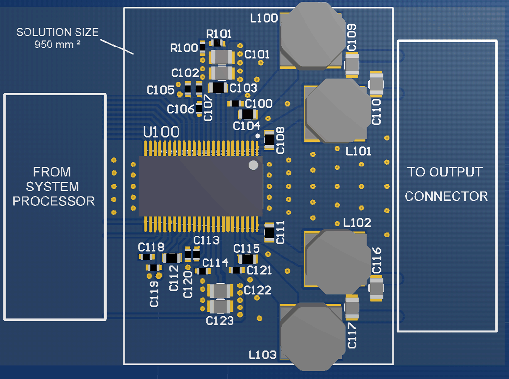 Figure 85. 2.0 (Stereo BTL) 3-D View
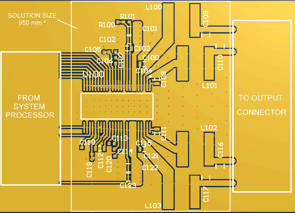 Figure 86. 2.0 (Stereo BTL) Top Copper View
11.2.2 Mono (PBTL) System
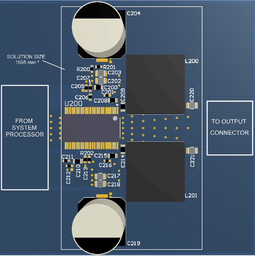 Figure 87. Mono (PBTL) 3-D View
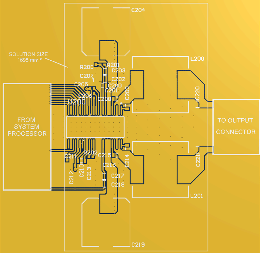 Figure 88. Mono (PBTL) Top Copper View
11.2.3 2.1 (Stereo BTL + Mono PBTL) Systems
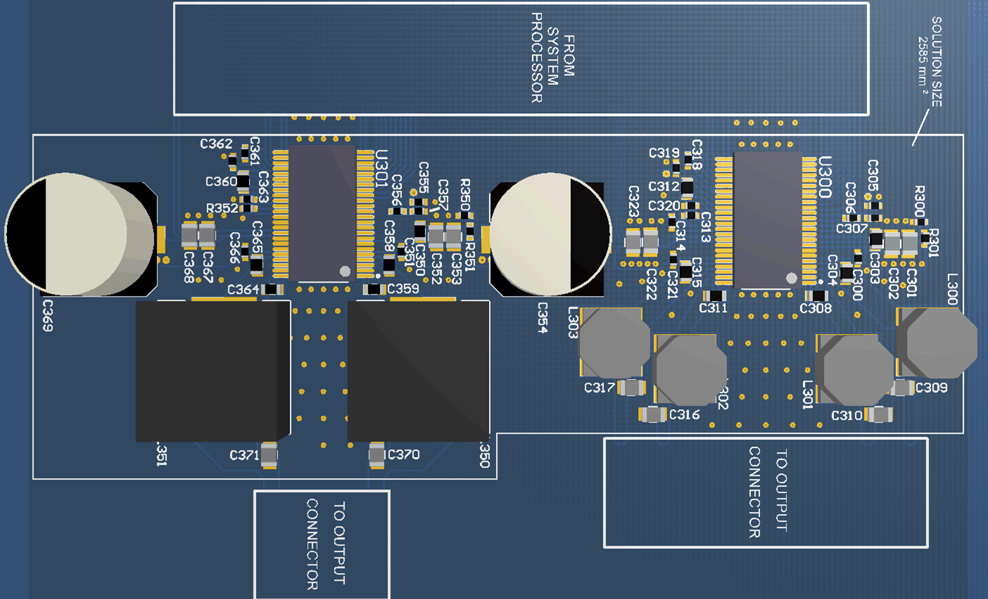 Figure 89. 2.1 (Stereo BTL + Mono PBTL) 3-D View
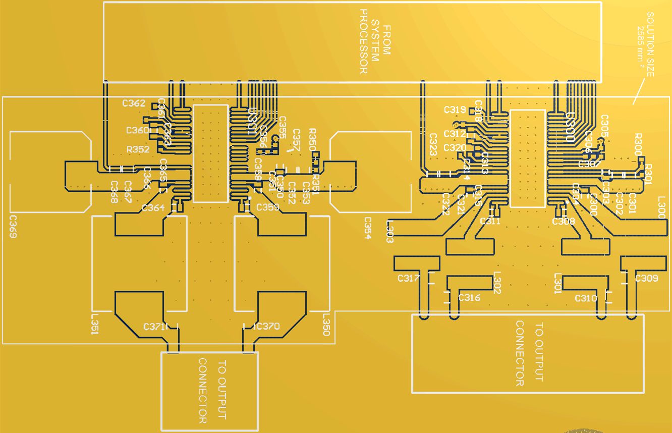 Figure 90. 2.1 (Stereo BTL + Mono PBTL) Top Copper View
11.2.4 2.2 (Dual Stereo BTL) Systems
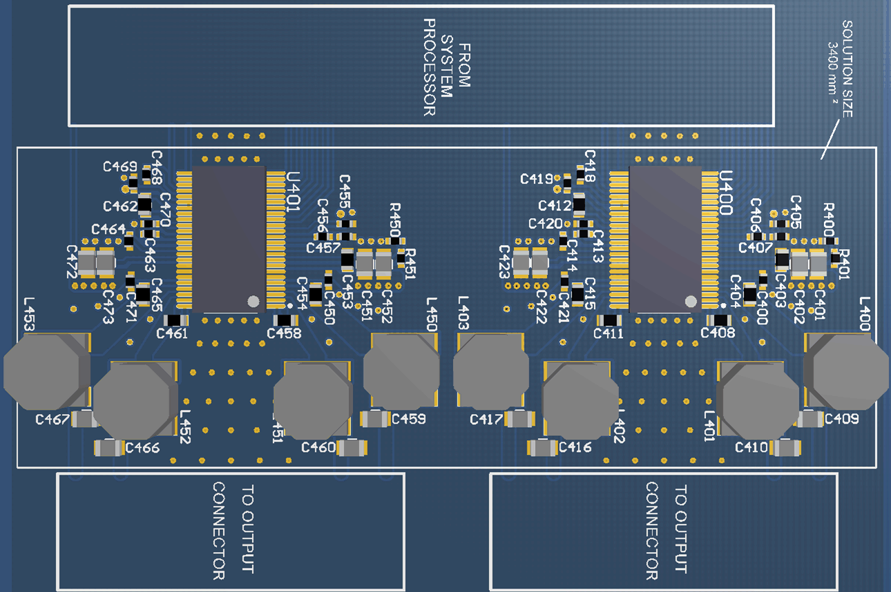 Figure 91. 2.2 (Dual Stereo BTL) 3-D View
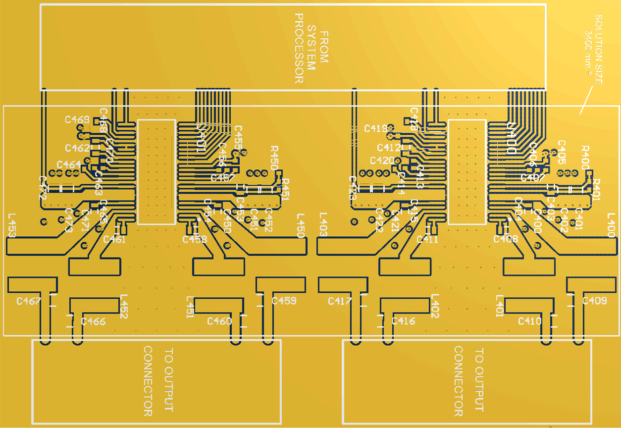 Figure 92. 2.2 (Dual Stereo BTL) Top Copper View
11.2.5 1.1 (Bi-Amped BTL) Systems
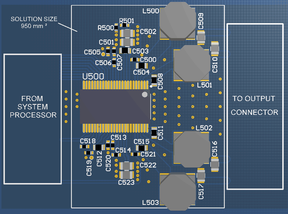 Figure 93. 1.1 (Bi-Amped BTL) 3-D View
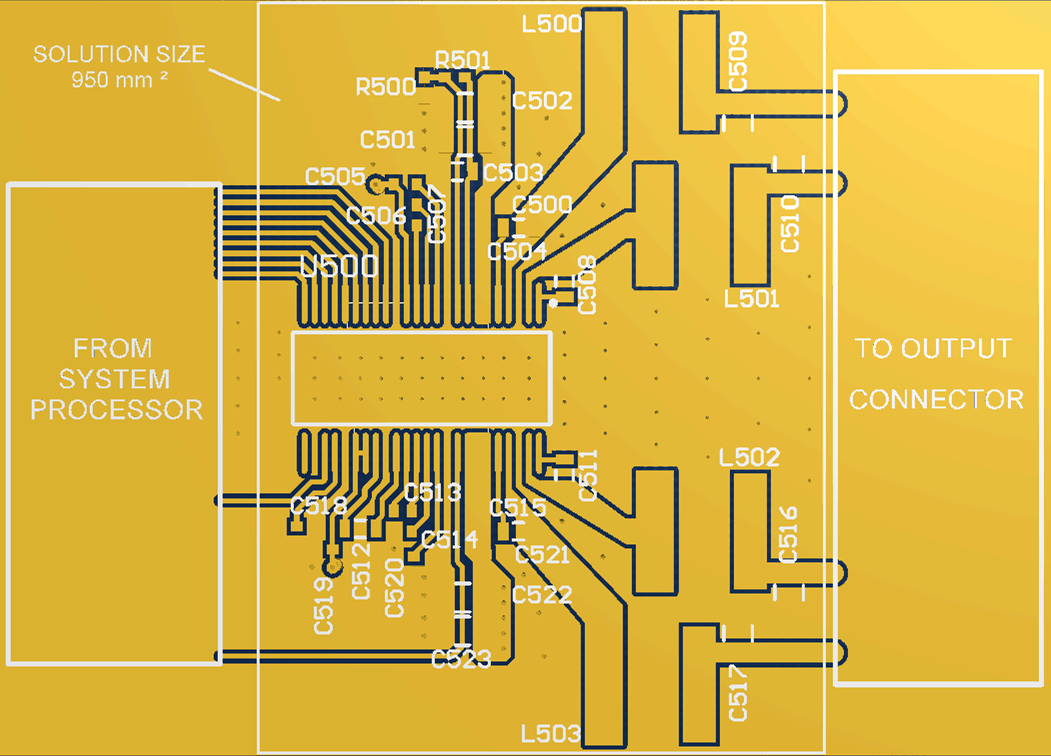 Figure 94. 2. 1.1 (Bi-Amped BTL) Top Copper View