SLAS988B June 2014 – August 2015 TAS5756M
PRODUCTION DATA.
- 1 Features
- 2 Applications
- 3 Description
- 4 Revision History
- 5 Device Comparison Table
- 6 Pin Configuration and Functions
-
7 Specifications
- 7.1 Absolute Maximum Ratings
- 7.2 ESD Ratings
- 7.3 Recommended Operating Conditions
- 7.4 Thermal Information
- 7.5 Electrical Characteristics
- 7.6 MCLK Timing
- 7.7 Serial Audio Port Timing - Slave Mode
- 7.8 Serial Audio Port Timing - Master Mode
- 7.9 I2C Bus Timing - Standard
- 7.10 I2C Bus Timing - Fast
- 7.11 SPK_MUTE Timing
- 7.12 Power Dissipation
- 7.13 Typical Characteristics
-
8 Detailed Description
- 8.1 Overview
- 8.2 Functional Block Diagram
- 8.3
Feature Description
- 8.3.1 Power-on-Reset (POR) Function
- 8.3.2 Device Clocking
- 8.3.3
Serial Audio Port
- 8.3.3.1 Clock Master Mode from Audio Rate Master Clock
- 8.3.3.2 Clock Master from a Non-Audio Rate Master Clock
- 8.3.3.3 Clock Slave Mode with 4-Wire Operation (SCLK, MCLK, LRCK/FS, SDIN)
- 8.3.3.4 Clock Slave Mode with SLCK PLL to Generate Internal Clocks (3-Wire PCM)
- 8.3.3.5 Serial Audio Port - Data Formats and Bit Depths
- 8.3.3.6 Input Signal Sensing (Power-Save Mode)
- 8.3.3.7 Serial Data Output
- 8.3.4 Modulation Scheme
- 8.3.5 miniDSP Audio Processing Engine
- 8.3.6 Adjustable Amplifier Gain and Switching Frequency Selection
- 8.3.7
Error Handling and Protection Suite
- 8.3.7.1 Device Overtemperature Protection
- 8.3.7.2 SPK_OUTxx Overcurrent Protection
- 8.3.7.3 DC Offset Protection
- 8.3.7.4 Internal VAVDD Undervoltage-Error Protection
- 8.3.7.5 Internal VPVDD Undervoltage-Error Protection
- 8.3.7.6 Internal VPVDD Overvoltage-Error Protection
- 8.3.7.7 External Undervoltage-Error Protection
- 8.3.7.8 Internal Clock Error Notification (CLKE)
- 8.3.8 GPIO Port and Hardware Control Pins
- 8.3.9 I2C Communication Port
- 8.4 Device Functional Modes
-
9 Application and Implementation
- 9.1 Application Information
- 9.2
Typical Applications
- 9.2.1 2.0 (Stereo BTL) System
- 9.2.2 Mono (PBTL) Systems
- 9.2.3 2.1 (Stereo BTL + External Mono Amplifier) Systems
- 9.2.4 2.2 (Dual Stereo BTL) Systems
- 9.2.5 1.1 (Dual BTL, Bi-Amped) Systems
- 10Power Supply Recommendations
- 11Layout
- 12Device and Documentation Support
- 13Mechanical, Packaging, and Orderable Information
パッケージ・オプション
メカニカル・データ(パッケージ|ピン)
- DCA|48
サーマルパッド・メカニカル・データ
- DCA|48
発注情報
7 Specifications
7.1 Absolute Maximum Ratings
over operating free-air temperature range (unless otherwise noted)(1)| MIN | MAX | UNIT | ||
|---|---|---|---|---|
| Low-voltage digital, analog, charge pump supply | DVDD, AVDD, CPVDD | –0.3 | 3.9 | V |
| PVDD supply | PVDD | –0.3 | 30 | V |
| Input voltage for SPK_GAIN/FREQ and SPK_FAULT pins | VI(AmpCtrl) | –0.3 | VGVDD + 0.3 | V |
| DVDD referenced digital inputs(2) | VI(DigIn) | –0.5 | VDVDD + 0.5 | V |
| Analog input into speaker amplifier | VI(SPK_INxx) | –0.3 | 6.3 | V |
| Voltage at speaker output pins | VI(SPK_OUTxx) | –0.3 | 32 | V |
| Ambient operating temperature, TA | –25 | 85 | °C | |
| Storage temperature, Tstg | –40 | 125 | °C | |
(1) Stresses beyond those listed under absolute maximum ratings may cause permanent damage to the device. These are stress ratings only, and functional operation of the device at these or any other conditions beyond those indicated under recommended operating conditions is not implied. Exposure to absolute-maximum-rated conditions for extended periods may affect device reliability.
(2) DVDD referenced digital pins include: ADR0, ADR1, GPIO0, GPIO1, GPIO2, LRCK/FS, MCLK, SCL, SCLK, SDA, SDIN, and SPK_MUTE.
7.2 ESD Ratings
| VALUE | UNIT | |||
|---|---|---|---|---|
| V(ESD) | Electrostatic discharge | Human-body model (HBM), per ANSI/ESDA/JEDEC JS-001(1) | ±2000 | V |
| Charged-device model (CDM), per JEDEC specification JESD22-C101(2) | ±500 | |||
(1) JEDEC document JEP155 states that 2000-V HBM allows safe manufacturing with a standard ESD control process.
(2) JEDEC document JEP157 states that 500-V CDM allows safe manufacturing with a standard ESD control process.
7.3 Recommended Operating Conditions
over operating free-air temperature range (unless otherwise noted)| MIN | NOM | MAX | UNIT | |||
|---|---|---|---|---|---|---|
| V(POWER) | Power supply inputs | DVDD, AVDD, CPVDD | 2.9 | 3.63 | V | |
| PVDD | 4.5 | 26.4 | ||||
| RSPK | Minimum speaker load | BTL Mode | 3 | Ω | ||
| PBTL Mode | 2 | Ω | ||||
| VIH(DigIn) | Input logic high for DVDD referenced digital inputs(2)(1) | 0.9 × VDVDD | VDVDD | V | ||
| VIL(DigIn) | Input logic low for DVDD referenced digital inputs(2)(2) | VDVDD | 0 | 0.1 × VDVDD | V | |
| LOUT | Minimum inductor value in LC filter under short-circuit condition | 1 | 4.7 | µH | ||
(1) The best practice for driving the input pins of the TAS5756M device is to power the drive circuit or pullup resistor from the same supply which provides the DVDD power supply.
(2) The best practice for driving the input pins of the TAS5756M device low is to pull them down, either actively or through pulldown resistors to the system ground.
7.4 Thermal Information
| THERMAL METRIC(1)(2) | TAS5756M DCA (HTSSOP) 48 PINS |
UNIT | |||
|---|---|---|---|---|---|
| JEDEC STANDARD 2-LAYER PCB |
JEDEC STANDARD 4-LAYER PCB |
TAS5756MDCAEVM 4-LAYER PCB |
|||
| RθJA | Junction-to-ambient thermal resistance | 41.8 | 27.6 | 19.4 | °C/W |
| RθJC(top) | Junction-to-case (top) thermal resistance | 14.4 | 14.4 | 14.4 | °C/W |
| RθJB | Junction-to-board thermal resistance | 9.4 | 9.4 | 9.4 | °C/W |
| ψJT | Junction-to-top characterization parameter | 0.6 | 0.6 | 2 | °C/W |
| ψJB | Junction-to-board characterization parameter | 8.1 | 9.3 | 4.8 | °C/W |
| RθJC(bot) | Junction-to-case (bottom) thermal resistance | 1 | 1 | N/A | °C/W |
(1) For more information about traditional and new thermal metrics, see the Semiconductor and IC Package Thermal Metrics application report, SPRA953.
(2) For the PCB layout, see the Using the TAS5754/6M HybridFlow Processor user's guide, SLAU577.
7.5 Electrical Characteristics
over operating free-air temperature range (unless otherwise noted)| PARAMETER | TEST CONDITIONS | MIN | TYP | MAX | UNIT | |
|---|---|---|---|---|---|---|
| DIGITAL I/O | ||||||
| |IIH|1 | Input logic high current level for DVDD referenced digital input pins(2) | VIN(DigIn) = VDVDD | 10 | µA | ||
| |IIL|1 | Input logic low current level for DVDD referenced digital input pins(2) | VIN(DigIn) = 0 V | –10 | µA | ||
| VIH1 | Input logic high threshold for DVDD referenced digital inputs(2) | 70% | VDVDD | |||
| VIL1 | Input logic low threshold for DVDD referenced digital inputs(2) | 30% | VDVDD | |||
| VOH(DigOut) | Output logic high voltage level(2) | IOH = 4 mA | 80% | VDVDD | ||
| VOL(DigOut) | Output logic low voltage level(2) | IOH = –4 mA | 22% | VDVDD | ||
| VOL(SPK_FAULT) | Output logic low voltage level for SPK_FAULT | With 100-kΩ pullup resistor | 0.8 | V | ||
| I2C CONTROL PORT | ||||||
| CL(I2C) | Allowable load capacitance for each I2C Line | 400 | pF | |||
| fSCL(fast) | Support SCL frequency | No wait states, fast mode | 400 | kHz | ||
| fSCL(slow) | Support SCL frequency | No wait states, slow mode | 100 | kHz | ||
| VNH | Noise margin at High level for each connected device (including hysteresis) | 0.2 × VDD | V | |||
| MCLK AND PLL SPECIFICATIONS | ||||||
| DMCLK | Allowable MCLK duty cycle | 40% | 60% | |||
| fMCLK | Supported MCLK frequencies | Up to 50 MHz | 128 | 512 | fS(1) | |
| fPLL | PLL input frequency | Clock divider uses fractional divide D > 0, P = 1 |
6.7 | 20 | MHz | |
| Clock divider uses integer divide D = 0, P = 1 |
1 | 20 | ||||
| SERIAL AUDIO PORT | ||||||
| tDLY | Required LRCK/FS to SCLK rising edge delay | 5 | ns | |||
| DSCLK | Allowable SCLK duty cycle | 40% | 60% | |||
| fS | Supported input sample rates | 8 | 192 | kHz | ||
| fSCLK | Supported SCLK frequencies | 32 | 64 | fS(1) | ||
| fSCLK | SCLK frequency | Either master mode or slave mode | 24.576 | MHz | ||
| SPEAKER AMPLIFIER (ALL OUTPUT CONFIGURATIONS) | ||||||
| AV(SPK_AMP) | Speaker amplifier gain | SPK_GAIN/FREQ voltage < 3 V, see Adjustable Amplifier Gain and Switching Frequency Selection |
20 | dBV | ||
| SPK_GAIN/FREQ voltage > 3.3 V, see Adjustable Amplifier Gain and Switching Frequency Selection |
26 | dBV | ||||
| ΔAV(SPK_AMP) | Typical variation of speaker amplifier gain | ±1 | dBV | |||
| fSPK_AMP | Switching frequency of the speaker amplifier | Switching frequency depends on voltage presented at SPK_GAIN/FREQ pin and the clocking arrangement, including the incoming sample rate, see Adjustable Amplifier Gain and Switching Frequency Selection | 176.4 | 768 | kHz | |
| KSVR | Power supply rejection ratio | Injected Noise = 50 Hz to 60 Hz, 200 mVP-P, Gain = 26 dBV, input audio signal = digital zero | 60 | dB | ||
| rDS(on) | Drain-to-source on resistance of the individual output MOSFETs | VPVDD = 24 V, I(SPK_OUT) = 500 mA, TJ = 25°C, includes PVDD/PGND pins, leadframe, bondwires and metallization layers. | 90 | mΩ | ||
| VPVDD = 24 V, I(SPK_OUT) = 500 mA, TJ = 25°C | 90 | mΩ | ||||
| OCETHRES | SPK_OUTxx Overcurrent Error Threshold | 7.5 | A | |||
| OTETHRES | Overtemperature Error Threshold | 150 | °C | |||
| OCECLRTIME | Time required to clear Overcurrent Error after error condition is removed. | 1.3 | s | |||
| OTECLRTIME | Time required to clear Overtemperature Error after error condition is removed. | 1.3 | s | |||
| OVETHRES(PVDD) | PVDD Overvoltage Error Threshold | 27 | V | |||
| UVETHRES(PVDD) | PVDD Undervoltage Error Threshold | 4.5 | V | |||
| SPEAKER AMPLIFIER (STEREO BTL) | ||||||
| |VOS| | Amplifier offset voltage | Measured differentially with zero input data, SPK_GAIN/FREQ pin configured for 20 dBV gain, VPVDD = 12 V | 2 | 10 | mV | |
| Measured differentially with zero input data, SPK_GAIN/FREQ pin configured for 26 dBV gain, VPVDD = 24 V | 6 | 15 | ||||
| ICN(SPK) | Idle channel noise | VPVDD = 12 V, SPK_GAIN = 20 dBV, RSPK = 8 Ω, A-Weighted | 56 | µVRMS | ||
| VPVDD = 15 V, SPK_GAIN = 20 dBV, RSPK = 8 Ω, A-Weighted | 58 | |||||
| VPVDD = 19 V, SPK_GAIN = 26 dBV, RSPK = 8 Ω, A-Weighted | 86 | |||||
| VPVDD = 24 V, SPK_GAIN = 26 dBV, RSPK = 8 Ω, A-Weighted | 88 | |||||
| PO(SPK) | Output Power (Per Channel) | VPVDD = 12 V, SPK_GAIN = 20 dBV, RSPK = 4 Ω, THD+N = 0.1%, Unless otherwise noted | 15 | W | ||
| VPVDD = 24 V, SPK_GAIN = 26 dBV, RSPK = 4 Ω, THD+N = 0.1%, Unless otherwise noted | 20 | |||||
| VPVDD = 24 V, SPK_GAIN = 26 dBV, RSPK = 8 Ω, THD+N = 0.1% | 28 | |||||
| VPVDD = 12 V, SPK_GAIN = 20 dBV, RSPK = 8 Ω, THD+N = 0.1% | 20 | |||||
| VPVDD = 19 V, SPK_GAIN = 26 dBV, RSPK = 4 Ω, THD+N = 0.1%, Unless otherwise noted | 18 | |||||
| VPVDD = 19 V, SPK_GAIN = 26 dBV, RSPK = 8 Ω, THD+N = 0.1% | 18 | |||||
| VPVDD = 15 V, SPK_GAIN = 26 dBV, RSPK = 4 Ω, THD+N = 0.1%, Unless otherwise noted | 18 | |||||
| VPVDD = 15 V, SPK_GAIN = 26 dBV, RSPK = 8 Ω, THD+N = 0.1% | 12 | |||||
| SNR | Signal-to-noise ratio (referenced to 0 dBFS input signal) | VPVDD = 15 V, SPK_GAIN = 26 dBV, RSPK = 8 Ω, A-Weighted, –120 dBFS Input | 104 | dB | ||
| VPVDD = 12 V, SPK_GAIN = 20 dBV, RSPK = 8 Ω, A-Weighted, –120 dBFS Input | 104 | |||||
| VPVDD = 24 V, SPK_GAIN = 26 dBV, RSPK = 8 Ω, A-Weighted, –120 dBFS Input | 106 | |||||
| VPVDD = 19 V, SPK_GAIN = 26 dBV, RSPK = 8 Ω, A-Weighted, –120 dBFS Input | 105 | |||||
| THD+NSPK | Total harmonic distortion and noise | VPVDD = 12 V, SPK_GAIN = 20 dBV, RSPK = 4 Ω, PO = 1 W | 0.011% | |||
| VPVDD = 12 V, SPK_GAIN = 20 dBV, RSPK = 8 Ω, PO = 1 W | 0.007% | |||||
| VPVDD = 24 V, SPK_GAIN = 26 dBV, RSPK = 4 Ω, PO = 1 W | 0.02% | |||||
| VPVDD = 15 V, SPK_GAIN = 26 dBV, RSPK = 4 Ω, PO = 1 W | 0.015% | |||||
| VPVDD = 15 V, SPK_GAIN = 26 dBV, RSPK = 8 Ω, PO = 1 W | 0.01% | |||||
| VPVDD = 19 V, SPK_GAIN = 26 dBV, RSPK = 4 Ω, PO = 1 W | 0.017% | |||||
| VPVDD = 19 V, SPK_GAIN = 26 dBV, RSPK = 8 Ω, PO = 1 W | 0.015% | |||||
| VPVDD = 24 V, SPK_GAIN = 26 dBV, RSPK = 8 Ω, PO = 1 W | 0.017% | |||||
| X-talkSPK | Cross-talk (worst case between left-to-right and right-to-left coupling) | VPVDD = 15 V, SPK_GAIN = 26 dBV, RSPK = 8 Ω, Input Signal 250 mVrms, 1-kHz Sine, across f(S) |
–88 | dB | ||
| VPVDD = 12 V, SPK_GAIN = 20 dBV, RSPK = 8 Ω, Input Signal 250 mVrms, 1-kHz Sine, across f(S) |
–97 | |||||
| VPVDD = 24 V, SPK_GAIN = 26 dBV, RSPK = 8 Ω, Input Signal 250 mVrms, 1-kHz Sine, across f(S) |
–88 | |||||
| VPVDD = 19 V, SPK_GAIN = 26 dBV, RSPK = 8 Ω, Input Signal 250 mVrms, 1-kHz Sine, across f(S) |
–88 | |||||
| SPEAKER AMPLIFIER (MONO PBTL) | ||||||
| |VOS| | Amplifier offset voltage | Measured differentially with zero input data, SPK_GAIN/FREQ pin configured for 20 dBV gain, VPVDD = 12 V | 0.5 | 8 | mV | |
| Measured differentially with zero input data, SPK_GAIN/FREQ pin configured for 26 dBV gain, VPVDD = 24 V | 1 | 14 | ||||
| ICN | Idle channel noise | VPVDD = 15 V, SPK_GAIN = 20 dBV, RSPK = 8 Ω, A-Weighted | 58 | µVRMS | ||
| VPVDD = 12 V, SPK_GAIN = 20 dBV, RSPK = 8 Ω, A-Weighted | 57 | |||||
| VPVDD = 19 V, SPK_GAIN = 26 dBV, RSPK = 8 Ω, A-Weighted | 85 | |||||
| VPVDD = 24 V, SPK_GAIN = 26 dBV, RSPK = 8 Ω, A-Weighted | 85 | |||||
| PO | Output Power (Per Channel) | VPVDD = 24 V, SPK_GAIN = 26 dBV, RSPK = 2 Ω, THD+N = 0.1%, Unless otherwise noted | 40 | W | ||
| VPVDD = 24 V, SPK_GAIN = 26 dBV, RSPK = 4 Ω, THD+N = 0.1%, Unless otherwise noted | 56 | |||||
| VPVDD = 24 V, SPK_GAIN = 26 dBV, RSPK = 8 Ω, THD+N = 0.1% | 34 | |||||
| VPVDD = 19 V, SPK_GAIN = 26 dBV, RSPK = 2 Ω, THD+N = 0.1%, Unless otherwise noted | 40 | |||||
| VPVDD = 12 V, SPK_GAIN = 20 dBV, RSPK = 8 Ω, THD+N = 0.1% | 8 | |||||
| VPVDD = 19 V, SPK_GAIN = 26 dBV, RSPK = 4 Ω, THD+N = 0.1%, Unless otherwise noted | 36 | |||||
| VPVDD = 19 V, SPK_GAIN = 26 dBV, RSPK = 8 Ω, THD+N = 0.1% | 21.3 | |||||
| VPVDD = 15 V, SPK_GAIN = 26 dBV, RSPK = 2 Ω, THD+N = 0.1%, Unless otherwise noted | 36 | |||||
| VPVDD = 15 V, SPK_GAIN = 26 dBV, RSPK = 4 Ω, THD+N = 0.1%, Unless otherwise noted | 24 | |||||
| VPVDD = 15 V, SPK_GAIN = 26 dBV, RSPK = 8 Ω, THD+N = 0.1% | 13.5 | |||||
| VPVDD = 12 V, SPK_GAIN = 20 dBV, RSPK = 2 Ω, THD+N = 0.1%, Unless otherwise noted | 30 | |||||
| VPVDD = 12 V, SPK_GAIN = 20 dBV, RSPK = 4 Ω, THD+N = 0.1%, Unless otherwise noted | 15 | |||||
| SNR | Signal-to-noise ratio (referenced to 0 dBFS input signal) |
VPVDD = 15 V, SPK_GAIN = 26 dBV, RSPK = 8 Ω, A-Weighted, –120 dBFS Input | 104 | dB | ||
| VPVDD = 12 V, SPK_GAIN = 20 dBV, RSPK = 8 Ω, A-Weighted, –120 dBFS Input | 104 | |||||
| VPVDD = 24 V, SPK_GAIN = 26 dBV, RSPK = 8 Ω, A-Weighted, –120 dBFS Input | 107 | |||||
| VPVDD = 19 V, SPK_GAIN = 26 dBV, RSPK = 8 Ω, A-Weighted, –120 dBFS Input | 105 | |||||
| THD+N | Total harmonic distortion and noise | VPVDD = 12 V, SPK_GAIN = 20 dBV, RSPK = 4 Ω, PO = 1 W | 0.013% | |||
| VPVDD = 12 V, SPK_GAIN = 20 dBV, RSPK = 8 Ω, PO = 1 W | 0.007% | |||||
| VPVDD = 24 V, SPK_GAIN = 26 dBV, RSPK = 4 Ω, PO = 1 W | 0.02% | |||||
| VPVDD = 24 V, SPK_GAIN = 26 dBV, RSPK = 2 Ω, PO = 1 W | 0.028% | |||||
| VPVDD = 24 V, SPK_GAIN = 26 dBV, RSPK = 8 Ω, PO = 1 W | 0.018% | |||||
| VPVDD = 19 V, SPK_GAIN = 26 dBV, RSPK = 4 Ω, PO = 1 W | 0.017% | |||||
| VPVDD = 19 V, SPK_GAIN = 26 dBV, RSPK = 2 Ω, PO = 1 W | 0.027% | |||||
| VPVDD = 15 V, SPK_GAIN = 26 dBV, RSPK = 4 Ω, PO = 1 W | 0.016% | |||||
| VPVDD = 15 V, SPK_GAIN = 26 dBV, RSPK = 2 Ω, PO = 1 W | 0.03% | |||||
| VPVDD = 15 V, SPK_GAIN = 26 dBV, RSPK = 8 Ω, PO = 1 W | 0.01% | |||||
| VPVDD = 12 V, SPK_GAIN = 20 dBV, RSPK = 2 Ω, PO = 1 W | 0.03% | |||||
| VPVDD = 19 V, SPK_GAIN = 26 dBV, RSPK = 8 Ω, PO = 1 W | 0.012% | |||||
(1) A unit of fS indicates that the specification is the value listed in the table multiplied by the sample rate of the audio used in the TAS5756M device.
(2) DVDD referenced digital pins include: ADR0, ADR1, GPIO0, GPIO1, GPIO2, LRCK/FS, MCLK, SCL, SCLK, SDA, SDIN, and SPK_MUTE.
7.6 MCLK Timing
See Figure 18.| MIN | NOM | MAX | UNIT | ||
|---|---|---|---|---|---|
| tMCLK | MCLK period | 20 | 1000 | ns | |
| tMCLKH | MCLK pulse width, high | 9 | ns | ||
| tMCLKL | MCLK pulse width, low | 9 | ns | ||
7.7 Serial Audio Port Timing – Slave Mode
See Figure 19.| MIN | NOM | MAX | UNIT | ||
|---|---|---|---|---|---|
| fSCLK | SCLK frequency | 1.024 | MHz | ||
| tSCLK | SCLK period | 40 | ns | ||
| tSCLKL | SCLK pulse width, low | 16 | ns | ||
| tSCLKH | SCLK pulse width, high | 16 | ns | ||
| tSL | SCLK rising to LRCK/FS edge | 8 | ns | ||
| tLS | LRCK/FS Edge to SCLK rising edge | 8 | ns | ||
| tSU | Data setup time, before SCLK rising edge | 8 | ns | ||
| tDH | Data hold time, after SCLK rising edge | 8 | ns | ||
| tDFS | Data delay time from SCLK falling edge | 15 | ns | ||
7.8 Serial Audio Port Timing – Master Mode
See Figure 20.| MIN | NOM | MAX | UNIT | ||
|---|---|---|---|---|---|
| tSCLK | SCLK period | 40 | ns | ||
| tSCLKL | SCLK pulse width, low | 16 | ns | ||
| tSCLKH | SCLK pulse width, high | 16 | ns | ||
| tLRD | LRCK/FS delay time from to SCLK falling edge | –10 | 20 | ns | |
| tSU | Data setup time, before SCLK rising edge | 8 | ns | ||
| tDH | Data hold time, after SCLK rising edge | 8 | ns | ||
| tDFS | Data delay time from SCLK falling edge | 15 | ns | ||
7.9 I2C Bus Timing – Standard
| MIN | MAX | UNIT | ||
|---|---|---|---|---|
| fSCL | SCL clock frequency | 100 | kHz | |
| tBUF | Bus free time between a STOP and START condition | 4.7 | µs | |
| tLOW | Low period of the SCL clock | 4.7 | µs | |
| tHI | High period of the SCL clock | 4 | µs | |
| tRS-SU | Setup time for (repeated) START condition | 4.7 | µs | |
| tS-HD | Hold time for (repeated) START condition | 4 | µs | |
| tD-SU | Data setup time | 250 | ns | |
| tD-HD | Data hold time | 0 | 900 | ns |
| tSCL-R | Rise time of SCL signal | 20 + 0.1CB | 1000 | ns |
| tSCL-R1 | Rise time of SCL signal after a repeated START condition and after an acknowledge bit | 20 + 0.1CB | 1000 | ns |
| tSCL-F | Fall time of SCL signal | 20 + 0.1CB | 1000 | ns |
| tSDA-R | Rise time of SDA signal | 20 + 0.1CB | 1000 | ns |
| tSDA-F | Fall time of SDA signal | 20 + 0.1CB | 1000 | ns |
| tP-SU | Setup time for STOP condition | 4 | µs | |
7.10 I2C Bus Timing – Fast
See Figure 21.| MIN | MAX | UNIT | ||
|---|---|---|---|---|
| fSCL | SCL clock frequency | 400 | kHz | |
| tBUF | Bus free time between a STOP and START condition | 1.3 | µs | |
| tLOW | Low period of the SCL clock | 1.3 | µs | |
| tHI | High period of the SCL clock | 600 | ns | |
| tRS-SU | Setup time for (repeated)START condition | 600 | ns | |
| tRS-HD | Hold time for (repeated)START condition | 600 | ns | |
| tD-SU | Data setup time | 100 | ns | |
| tD-HD | Data hold time | 0 | 900 | ns |
| tSCL-R | Rise time of SCL signal | 20 + 0.1CB | 300 | ns |
| tSCL-R1 | Rise time of SCL signal after a repeated START condition and after an acknowledge bit | 20 + 0.1CB | 300 | ns |
| tSCL-F | Fall time of SCL signal | 20 + 0.1CB | 300 | ns |
| tSDA-R | Rise time of SDA signal | 20 + 0.1CB | 300 | ns |
| tSDA-F | Fall time of SDA signal | 20 + 0.1CB | 300 | ns |
| tP-SU | Setup time for STOP condition | 600 | ns | |
| tSP | Pulse width of spike suppressed | 50 | ns | |
 Figure 18. Timing Requirements for MCLK Input
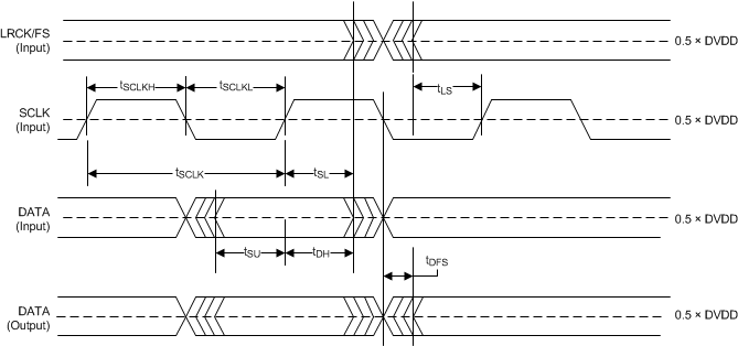 Figure 19. MCLK Timing Diagram in Slave Mode
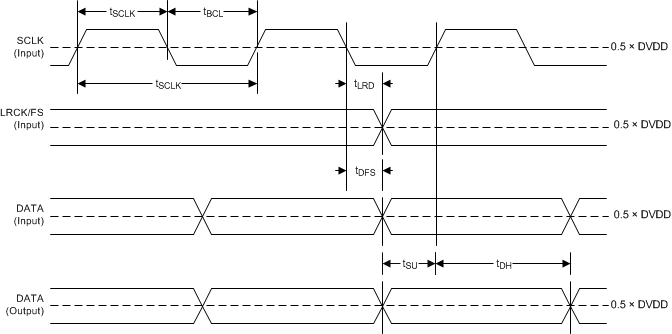 Figure 20. MCLK Timing Diagram in Master Mode
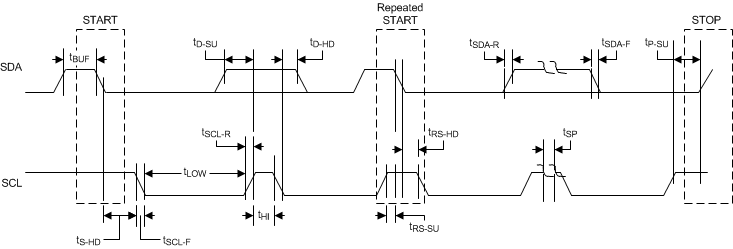 Figure 21. I2C Communication Port Timing Diagram
 Figure 22. SPK_MUTE Timing Diagram for Soft Mute Operation via Hardware Pin
7.12 Power Dissipation
| VPVDD
(V) |
SPK_GAIN(1)(2)(3)
(dBV) |
fSPK_AMP
(kHz) |
STATE OF OPERATION |
RSPK
(Ω) |
IPVDD(4)
(mA) |
IDVDD(5)
(mA) |
PDISS
(W) |
|---|---|---|---|---|---|---|---|
| 7.4 | 20 | 384 | Idle | 4 | 21.3 | 35 | 0.273 |
| 6 | 21.33 | 35 | 0.273 | ||||
| 8 | 21.3 | 35 | 0.273 | ||||
| Mute | 4 | 21.33 | 35 | 0.273 | |||
| 6 | 21.34 | 35 | 0.273 | ||||
| 8 | 21.36 | 35 | 0.274 | ||||
| Standby | 4 | 2.08 | 17 | 0.071 | |||
| 6 | 2.11 | 17 | 0.072 | ||||
| 8 | 2.17 | 17 | 0.072 | ||||
| Powerdown | 4 | 2.03 | 1 | 0.018 | |||
| 6 | 2.04 | 1 | 0.018 | ||||
| 8 | 2.06 | 1 | 0.019 | ||||
| 768 | Idle | 4 | 27.48 | 35 | 0.319 | ||
| 6 | 27.49 | 35 | 0.319 | ||||
| 8 | 24.46 | 35 | 0.297 | ||||
| Mute | 4 | 27.5 | 35 | 0.319 | |||
| 6 | 27.51 | 35 | 0.319 | ||||
| 8 | 27.52 | 35 | 0.319 | ||||
| Standby | 4 | 2.04 | 17 | 0.071 | |||
| 6 | 2.08 | 17 | 0.071 | ||||
| 8 | 2.11 | 17 | 0.072 | ||||
| Powerdown | 4 | 2.06 | 1 | 0.019 | |||
| 6 | 2.07 | 1 | 0.019 | ||||
| 8 | 2.08 | 1 | 0.019 | ||||
| 11.1 | 20 | 384 | Idle | 4 | 24.33 | 35 | 0.386 |
| 6 | 24.32 | 35 | 0.385 | ||||
| 8 | 24.36 | 35 | 0.386 | ||||
| Mute | 4 | 24.36 | 35 | 0.386 | |||
| 6 | 24.32 | 35 | 0.385 | ||||
| 8 | 24.37 | 35 | 0.386 | ||||
| Standby | 4 | 3.58 | 17 | 0.096 | |||
| 6 | 3.57 | 17 | 0.096 | ||||
| 8 | 3.58 | 17 | 0.096 | ||||
| Powerdown | 4 | 3.52 | 1 | 0.042 | |||
| 6 | 3.52 | 1 | 0.042 | ||||
| 8 | 3.54 | 1 | 0.043 | ||||
| 768 | Idle | 4 | 30.7 | 35 | 0.456 | ||
| 6 | 30.65 | 35 | 0.456 | ||||
| 8 | 30.67 | 35 | 0.456 | ||||
| Mute | 4 | 3.072 | 35 | 0.150 | |||
| 6 | 30.69 | 35 | 0.456 | ||||
| 8 | 30.69 | 35 | 0.456 | ||||
| Standby | 4 | 3.54 | 17 | 0.095 | |||
| 6 | 3.54 | 17 | 0.095 | ||||
| 8 | 3.58 | 17 | 0.096 | ||||
| Powerdown | 4 | 3.53 | 1 | 0.042 | |||
| 6 | 3.53 | 1 | 0.042 | ||||
| 8 | 3.55 | 1 | 0.043 | ||||
| 12 | 20 | 384 | Idle | 4 | 25.07 | 35 | 0.416 |
| 6 | 25.08 | 35 | 0.416 | ||||
| 8 | 25.1 | 35 | 0.417 | ||||
| Mute | 4 | 25.12 | 35 | 0.417 | |||
| 6 | 25.08 | 35 | 0.416 | ||||
| 8 | 25.11 | 35 | 0.417 | ||||
| Standby | 4 | 3.92 | 17 | 0.103 | |||
| 6 | 3.93 | 17 | 0.103 | ||||
| 8 | 3.94 | 17 | 0.103 | ||||
| Powerdown | 4 | 3.87 | 1 | 0.050 | |||
| 6 | 3.85 | 1 | 0.050 | ||||
| 8 | 3.87 | 1 | 0.050 | ||||
| 768 | Idle | 4 | 31.31 | 35 | 0.491 | ||
| 6 | 31.29 | 35 | 0.491 | ||||
| 8 | 31.31 | 35 | 0.491 | ||||
| Mute | 4 | 31.31 | 35 | 0.491 | |||
| 6 | 31.33 | 35 | 0.491 | ||||
| 8 | 31.32 | 35 | 0.491 | ||||
| Standby | 4 | 3.88 | 17 | 0.103 | |||
| 6 | 3.9 | 17 | 0.103 | ||||
| 8 | 3.91 | 17 | 0.103 | ||||
| Powerdown | 4 | 3.89 | 1 | 0.050 | |||
| 6 | 3.91 | 1 | 0.050 | ||||
| 8 | 3.88 | 1 | 0.050 | ||||
| 15 | 26 | 384 | Idle | 4 | 27.94 | 35 | 0.535 |
| 6 | 27.91 | 35 | 0.534 | ||||
| 8 | 27.75 | 35 | 0.532 | ||||
| Mute | 4 | 27.98 | 35 | 0.535 | |||
| 6 | 27.94 | 35 | 0.535 | ||||
| 8 | 27.88 | 35 | 0.534 | ||||
| Standby | 4 | 5.09 | 17 | 0.132 | |||
| 6 | 5.12 | 17 | 0.133 | ||||
| 8 | 5.19 | 17 | 0.134 | ||||
| Powerdown | 4 | 5.02 | 1 | 0.079 | |||
| 6 | 5.06 | 1 | 0.079 | ||||
| 8 | 5.14 | 1 | 0.080 | ||||
| 768 | Idle | 4 | 33.05 | 35 | 0.611 | ||
| 6 | 33.03 | 35 | 0.611 | ||||
| 8 | 33.08 | 35 | 0.612 | ||||
| Mute | 4 | 33.03 | 35 | 0.611 | |||
| 6 | 33.04 | 35 | 0.611 | ||||
| 8 | 33.05 | 35 | 0.611 | ||||
| Standby | 4 | 5.07 | 17 | 0.132 | |||
| 6 | 5.09 | 17 | 0.132 | ||||
| 8 | 5.14 | 17 | 0.133 | ||||
| Powerdown | 4 | 5.02 | 1 | 0.079 | |||
| 6 | 5.04 | 1 | 0.079 | ||||
| 8 | 5.09 | 1 | 0.080 | ||||
| 19.6 | 26 | 384 | Idle | 4 | 32.27 | 35 | 0.748 |
| 6 | 32.19 | 35 | 0.746 | ||||
| 8 | 32.08 | 35 | 0.744 | ||||
| Mute | 4 | 32.27 | 35 | 0.748 | |||
| 6 | 32.24 | 35 | 0.747 | ||||
| 8 | 32.22 | 35 | 0.747 | ||||
| Standby | 4 | 6.95 | 17 | 0.192 | |||
| 6 | 6.93 | 17 | 0.192 | ||||
| 8 | 7 | 17 | 0.193 | ||||
| Powerdown | 4 | 6.89 | 1 | 0.138 | |||
| 6 | 6.9 | 1 | 0.139 | ||||
| 8 | 6.96 | 1 | 0.140 | ||||
| 768 | Idle | 4 | 34.99 | 35 | 0.801 | ||
| 6 | 34.95 | 35 | 0.801 | ||||
| 8 | 34.97 | 35 | 0.801 | ||||
| Mute | 4 | 34.96 | 35 | 0.801 | |||
| 6 | 34.98 | 35 | 0.801 | ||||
| 8 | 34.96 | 35 | 0.801 | ||||
| Standby | 4 | 6.93 | 17 | 0.192 | |||
| 6 | 6.93 | 17 | 0.192 | ||||
| 8 | 6.98 | 17 | 0.193 | ||||
| Powerdown | 4 | 6.84 | 1 | 0.137 | |||
| 6 | 6.89 | 1 | 0.138 | ||||
| 8 | 6.9 | 1 | 0.139 | ||||
| 24 | 26 | 384 | Idle | 4 | 36.93 | 35 | 1.002 |
| 6 | 36.87 | 35 | 1.000 | ||||
| 8 | 36.77 | 35 | 0.998 | ||||
| Mute | 4 | 36.94 | 35 | 1.002 | |||
| 6 | 36.89 | 35 | 1.001 | ||||
| 8 | 36.85 | 35 | 1.000 | ||||
| Standby | 4 | 8.73 | 17 | 0.266 | |||
| 6 | 8.72 | 17 | 0.265 | ||||
| 8 | 8.71 | 17 | 0.265 | ||||
| Powerdown | 4 | 8.64 | 1 | 0.211 | |||
| 6 | 8.66 | 1 | 0.211 | ||||
| 8 | 8.69 | 1 | 0.212 | ||||
| 768 | Idle | 4 | 36.84 | 35 | 1.000 | ||
| 6 | 36.86 | 35 | 1.000 | ||||
| 8 | 36.83 | 35 | 0.999 | ||||
| Mute | 4 | 36.85 | 35 | 1.000 | |||
| 6 | 36.84 | 35 | 1.000 | ||||
| 8 | 36.82 | 35 | 0.999 | ||||
| Standby | 4 | 8.66 | 17 | 0.264 | |||
| 6 | 8.68 | 17 | 0.264 | ||||
| 8 | 8.71 | 17 | 0.265 | ||||
| Powerdown | 4 | 8.63 | 1 | 0.210 | |||
| 6 | 8.64 | 1 | 0.211 | ||||
| 8 | 8.65 | 1 | 0.211 |
(1) Mute: P0-R3-B0,B5 = 1
(2) Standby: P0-R2-B5 = 1
(3) P0-R2-B0 = 1
(4) IPVDD refers to all current that flows through the PVDD supply for the DUT. Any other current sinks not directly related to the DUT current draw were removed.
(5) IDVDD refers to all current that flows through the DVDD (3.3-V) supply for the DUT. Any other current sinks not directly related to the DUT current draw were removed.
7.13 Typical Characteristics
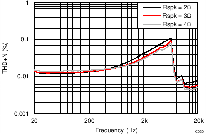
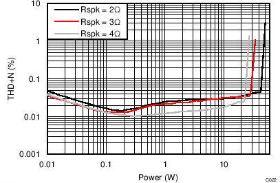
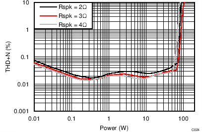
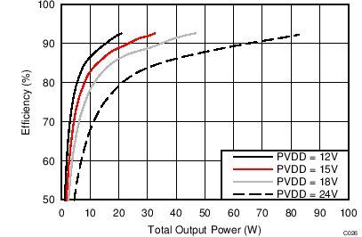
All performance plots were taken using the TAS5754M-56MEVM at room temperature, unless otherwise noted. The term Traditional LC filter refers to the output filter that is present by default on the EVM. For Filterless measurements, the on-board LC filter was removed and an Audio Precision AUX-025 measurement filter was used to take the measurements.
Table 1. Quick Reference Table
| OUTPUT CONFIGURATIONS |
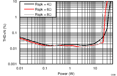
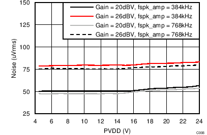
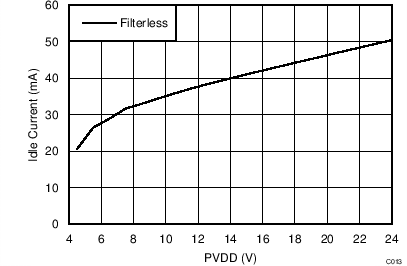
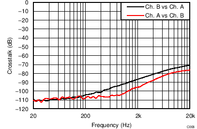
PLOT TITLE | FIGURE NUMBER |
|---|---|---|
| Bridge Tied Load (BTL) Configuration Curves | Output Power vs PVDD | Figure 23 |
| THD+N vs Frequency, VPVDD = 12 V | Figure 24 | |
| THD+N vs Frequency, VPVDD = 15 V | Figure 25 | |
| THD+N vs Frequency, VPVDD = 18 V | Figure 26 | |
| THD+N vs Frequency, VPVDD = 24 V | Figure 27 | |
| THD+N vs Power, VPVDD = 12 V | Figure 28 | |
| THD+N vs Power, VPVDD = 15 V | Figure 29 | |
| THD+N vs Power, VPVDD = 18 V | Figure 30 | |
| THD+N vs Power, VPVDD = 24 V | Figure 31 | |
| Idle Channel Noise vs PVDD | Figure 32 | |
| Efficiency vs Output Power | Figure 33 | |
| Idle Current Draw (Filterless) vs PVDD | Figure 34 | |
| Idle Current Draw (Traditional LC Filter) vs PVDD | Figure 35 | |
| Crosstalk vs. Frequency | Figure 36 | |
| PVDD PSRR vs Frequency | Figure 37 | |
| DVDD PSRR vs Frequency | Figure 38 | |
| AVDD PSRR vs Frequency | Figure 39 | |
| CPVDD PSRR vs Frequency | Figure 40 | |
| Powerdown Current Draw vs PVDD | Figure 41 | |
| Parallel Bridge Tied Load (PBTL) Configuration | Output Power vs PVDD | Figure 42 |
| THD+N vs Frequency, VPVDD = 12 V | Figure 43 | |
| THD+N vs Frequency, VPVDD = 15 V | Figure 44 | |
| THD+N vs Frequency, VPVDD = 18 V | Figure 45 | |
| THD+N vs Frequency, VPVDD = 24 V | Figure 46 | |
| THD+N vs Power, VPVDD = 12 V | Figure 47 | |
| THD+N vs Power, VPVDD = 15 V | Figure 48 | |
| THD+N vs Power, VPVDD = 18 V | Figure 49 | |
| THD+N vs Power, VPVDD = 24 V | Figure 50 | |
| Idle Channel Noise vs PVDD | Figure 51 | |
| Efficiency vs Output Power | Figure 52 | |
| Idle Current Draw (filterless) vs PVDD | Figure 57 | |
| Idle Current Draw (traditional LC filter) vs PVDD | Figure 58 | |
| PVDD PSRR vs Frequency | Figure 53 | |
| DVDD PSRR vs Frequency | Figure 54 | |
| AVDD PSRR vs Frequency | Figure 55 | |
| CPVDD PSRR vs Frequency | Figure 56 | |
| Powerdown Current Draw vs PVDD | Figure 59 |
7.13.1 Bridge Tied Load (BTL) Configuration Curves
Return to Quick Reference Table.
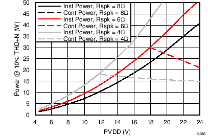
| AV(SPK_AMP) = 26 dBV |
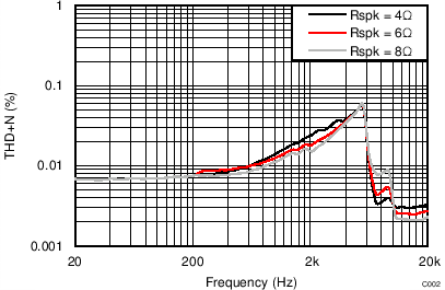
| AV(SPK_AMP) = 20 dBV | PO = 1 W | VPVDD = 15 V |
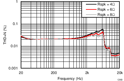
| AV(SPK_AMP)
= 26 dBV |
PO = 1 W | VPVDD = 24 V |
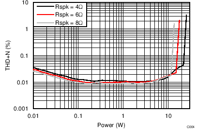
| AV(SPK_AMP)
= 20 dBV |
Input Signal = 1 kHz Sine | VPVDD = 15 V |
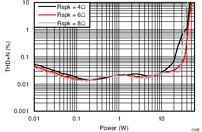
| AV(SPK_AMP) = 26 dBV | PO = 1 W | VPVDD = 24 V |
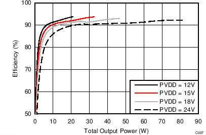
| RSPK = 8 Ω |
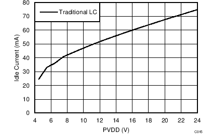
| fSPK_AMP = 768 kHz | RSPK = 8 Ω |
(Traditional LC Filter) vs PVDD – BTL
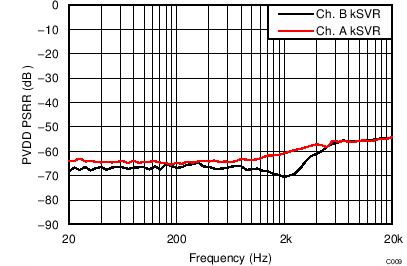
| AV(SPK_AMP) = 26 dBV | Supply Noise = 250 mV |
| VPVDD = 24 V | Sine Input |
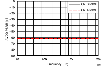
| AV(SPK_AMP) = 26 dBV | Supply Noise = 250 mV |
| VPVDD = 24 V | RSPK = 8 Ω |
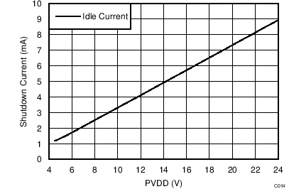
| AV(SPK_AMP) = 26 dBV | fSPK_AMP = 786 kHz | |
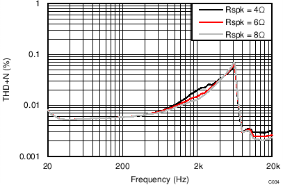
| AV(SPK_AMP) = 20 dBV | PO = 1 W | VPVDD = 12 V |
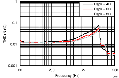
| AV(SPK_AMP) = 20 dBV | PO = 1 W | VPVDD = 18 V |
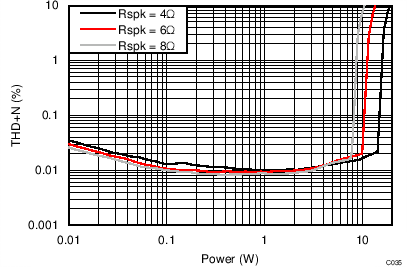
| AV(SPK_AMP)
= 20 dBV |
Input Signal = 1 kHz Sine | VPVDD = 12 V |
| AV(SPK_AMP)
= 26 dBV |
Input Signal = 1 kHz Sine | VPVDD = 18 V |
| AV(SPK_AMP) = 20 dBV | fSPK_AMP = 384 kHz | RSPK = 8 Ω |
| fSPK_AMP = 768 kHz | RSPK = 8 Ω |
| AV(SPK_AMP) = 26 dBV | Sine Input | VPVDD = 24 V |
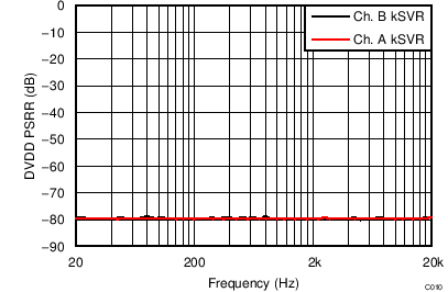
| AV(SPK_AMP) = 26 dBV | Supply Noise = 250 mV |
| VPVDD = 24 V | RSPK = 8 Ω |
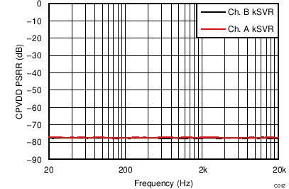
| AV(SPK_AMP) = 26 dBV | Supply Noise = 250 mV |
| VPVDD = 24 V | Sine Input |
7.13.2 Parallel Bridge Tied Load (PBTL) Configuration
Return to Quick Reference Table.
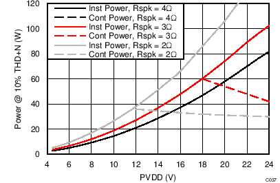
| AV(SPK_AMP) = 26 dBV | Measured on TAS5754/6 EVM | |
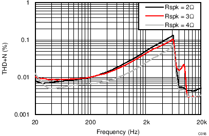
| AV(SPK_AMP) = 20 dBV | PO = 1 W | VPVDD = 15 V |
| AV(SPK_AMP) = 26 dBV | PO = 1 W | VPVDD = 24 V |
| AV(SPK_AMP) = 20 dBV |
PO = 1 W | VPVDD = 15 V |
| AV(SPK_AMP) = 20 dBV | PO = 1 W |
| VPVDD = 24 V | Input Signal = 1 kHz Sine |
| AV(SPK_AMP) = 26 dBV | ILOAD = xA | VPVDD = 24 V |
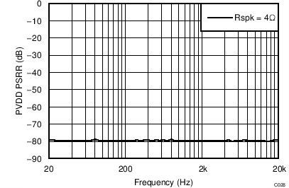
| AV(SPK_AMP) = 26 dBV | RSPK = 8 Ω |
| VPVDD = 24 V | Supply Noise = 250 mV |
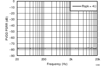
| AV(SPK_AMP) = 26 dBV | Sine Input |
| VPVDD = 24 V | Supply Noise = 250 mV |
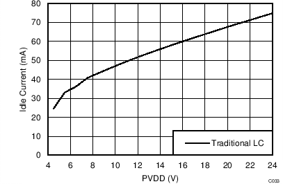
(Traditional LC filter) vs PVDD – PBTL
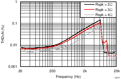
| AV(SPK_AMP) = 20 dBV | PO = 1 W | VPVDD = 12 V |
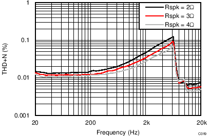
| AV(SPK_AMP) = 26 dBV | PO = 1 W | VPVDD = 18 V |
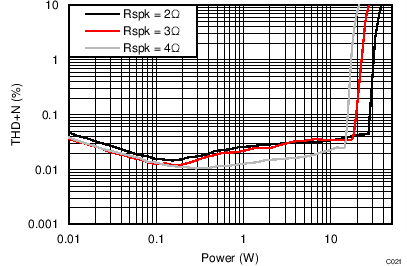
| AV(SPK_AMP) = 20 dBV | PO = 1 W | VPVDD = 12 V |
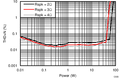
| AV(SPK_AMP) = 20 dBV | PO = 1 W |
| VPVDD = 18 V | Input Signal = 1 kHz Sine |
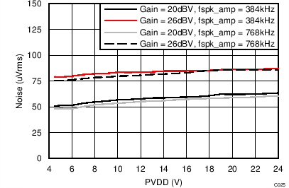
| AV(SPK_AMP)
= 26 dBV |
ILOAD = xA | VPVDD = 18 V |
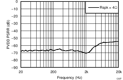
| AV(SPK_AMP) = 26dBV | Sine Input | VPVDD = 24V |
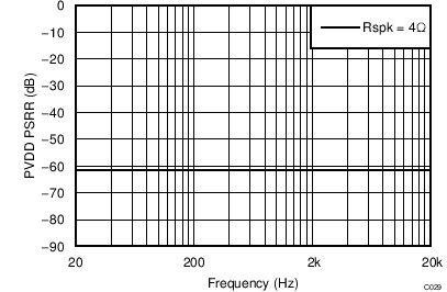
| AV(SPK_AMP) = 26 dBV | RSPK = 8 Ω |
| VPVDD = 24 V | Supply Noise = 250 mV |
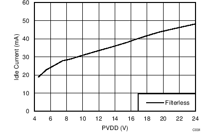
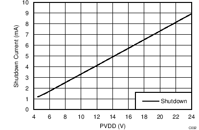
| AV(SPK_AMP) = 26 dBV | fSPK_AMP = 786 kHz |