JAJSHH5 May 2019 TAS5806MD
PRODUCTION DATA.
- 1 特長
- 2 アプリケーション
- 3 概要
- 4 改訂履歴
- 5 概要(続き)
- 6 Device Comparison Table
- 7 Pin Configuration and Functions
- 8 Specifications
- 9 Parametric Measurement Information
-
10Detailed Description
- 10.1 Overview
- 10.2 Functional Block Diagram
- 10.3 Feature Description
- 10.4 Device Functional Modes
- 10.5 Programming and Control
- 10.6
Register Maps
- 10.6.1
CONTROL PORT Registers
- 10.6.1.1 RESET_CTRL Register (Offset = 1h) [reset = 0x00]
- 10.6.1.2 DEVICE_CTRL_1 Register (Offset = 2h) [reset = 0x00]
- 10.6.1.3 DEVICE_CTRL_2 Register (Offset = 3h) [reset = 0x10]
- 10.6.1.4 I2C_PAGE_AUTO_INC Register (Offset = Fh) [reset = 0x00]
- 10.6.1.5 SIG_CH_CTRL Register (Offset = 28h) [reset = 0x00]
- 10.6.1.6 CLOCK_DET_CTRL Register (Offset = 29h) [reset = 0x00]
- 10.6.1.7 SDOUT_SEL Register (Offset = 30h) [reset = 0h]
- 10.6.1.8 I2S_CTRL Register (Offset = 31h) [reset = 0x00]
- 10.6.1.9 SAP_CTRL1 Register (Offset = 33h) [reset = 0x02]
- 10.6.1.10 SAP_CTRL2 Register (Offset = 34h) [reset = 0x00]
- 10.6.1.11 SAP_CTRL3 Register (Offset = 35h) [reset = 0x11]
- 10.6.1.12 FS_MON Register (Offset = 37h) [reset = 0x00]
- 10.6.1.13 BCK_MON Register (Offset = 38h) [reset = 0x00]
- 10.6.1.14 CLKDET_STATUS Register (Offset = 39h) [reset = 0x00]
- 10.6.1.15 CHANNEL_FORCE_HIZ Register (Offset = 40h) [reset = 0x01]
- 10.6.1.16 DIG_VOL_CTL Register (Offset = 4Ch) [reset = 30h]
- 10.6.1.17 DIG_VOL_CTRL2 Register (Offset = 4Eh) [reset = 0x33]
- 10.6.1.18 DIG_VOL_CTRL3 Register (Offset = 4Fh) [reset = 0x30]
- 10.6.1.19 AUTO_MUTE_CTRL Register (Offset = 50h) [reset = 0x07]
- 10.6.1.20 AUTO_MUTE_TIME Register (Offset = 51h) [reset = 0x00]
- 10.6.1.21 ANA_CTRL Register (Offset = 53h) [reset = 0x00]
- 10.6.1.22 AGAIN Register (Offset = 54h) [reset = 0x00]
- 10.6.1.23 BQ_WR_CTRL1 Register (Offset = 5Ch) [reset = 0x00]
- 10.6.1.24 DAC_CTRL Register (Offset = 5Dh) [reset = 0xF8]
- 10.6.1.25 ADR_PIN_CTRL Register (Offset = 60h) [reset = 0h]
- 10.6.1.26 ADR_PIN_CONFIG Register (Offset = 61h) [reset = 0x00]
- 10.6.1.27 DSP_MISC Register (Offset = 66h) [reset = 0h]
- 10.6.1.28 DIE_ID Register (Offset = 67h) [reset = 0h]
- 10.6.1.29 POWER_STATE Register (Offset = 68h) [reset = 0x00]
- 10.6.1.30 AUTOMUTE_STATE Register (Offset = 69h) [reset = 0x00]
- 10.6.1.31 PHASE_CTRL Register (Offset = 6Ah) [reset = 0x00]
- 10.6.1.32 SS_CTRL0 Register (Offset = 6Bh) [reset = 0x00]
- 10.6.1.33 SS_CTRL1 Register (Offset = 6Ch) [reset = 0x00]
- 10.6.1.34 SS_CTRL2 Register (Offset = 6Dh) [reset = 0x50]
- 10.6.1.35 SS_CTRL3 Register (Offset = 6Eh) [reset = 0x11]
- 10.6.1.36 SS_CTRL4 Register (Offset = 6Fh) [reset = 0x24]
- 10.6.1.37 CHAN_FAULT Register (Offset = 70h) [reset = 0x00]
- 10.6.1.38 GLOBAL_FAULT1 Register (Offset = 71h) [reset = 0h]
- 10.6.1.39 GLOBAL_FAULT2 Register (Offset = 72h) [reset = 0h]
- 10.6.1.40 OT WARNING Register (Offset = 73h) [reset = 0x00]
- 10.6.1.41 PIN_CONTROL1 Register (Offset = 74h) [reset = 0x00]
- 10.6.1.42 PIN_CONTROL2 Register (Offset = 75h) [reset = 0xF8]
- 10.6.1.43 MISC_CONTROL Register (Offset = 76h) [reset = 0x00]
- 10.6.1.44 HP_CONTROL Register (Offset = 77h) [reset = 0x00]
- 10.6.1.45 FAULT_CLEAR Register (Offset = 78h) [reset = 0x00]
- 10.6.1
CONTROL PORT Registers
- 11Application and Implementation
- 12Power Supply Recommendations
- 13Layout
- 14デバイスおよびドキュメントのサポート
- 15メカニカル、パッケージ、および注文情報
パッケージ・オプション
メカニカル・データ(パッケージ|ピン)
- DCP|38
サーマルパッド・メカニカル・データ
- DCP|38
発注情報
8.7.1 Bridge Tied Load (BTL) Configuration Curves with 1 SPW Mode
Free-air room temperature 25°C (unless otherwise noted) Measurements were made using TAS5806MDEVM board and Audio Precision System 2722 with Analog Analyzer filter set to 20-kHz brickwall filter. All measurements taken with audio frequency set to 1 kHz and device PWM Modulation mode set to 1 SPW mode with Class D Bandwidth =120 kHz for 576kHz Fsw and Class D Bandwidth = 175 kHz for 768 kHz Fsw (Listed in Register 0x53) unless otherwise noted.
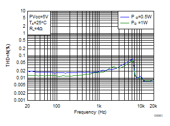
| PVDD = 5 V | 4.7 µH + 0.68 µF | |
| FSW = 576 kHz | 1 SPW Modulation | Load = 4 Ω |
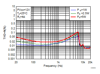
| PVDD = 12 V | 4.7 µH + 0.68 µF | |
| FSW = 768 kHz | 1SPW Modulation | Load = 4 Ω |
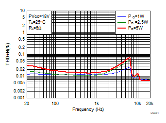
| PVDD = 18 V | 10 µH + 0.68 µF | |
| FSW = 768 kHz | 1SPW Modulation | Load = 6 Ω |
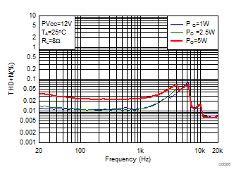
| PVDD = 12 V | 4.7 µH + 0.68 µF | |
| FSW = 768 kHz | 1SPW Modulation | Load = 8 Ω |
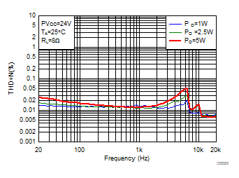
| PVDD = 24 V | 10 µH + 0.68 µF | |
| FSW = 768 kHz | 1SPW Modulation | Load = 8 Ω |
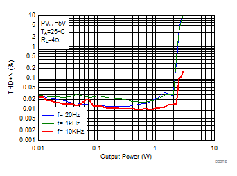
1.
Figure 11. THD+N vs Output Power-BTL | PVDD = 5 V | 1SPW Modulation | 4.7 µH + 0.68 µF |
| FSW = 768 kHz | Load = 4 Ω |
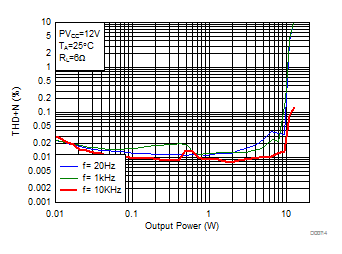
1.
Figure 13. THD+N vs Output Power-BTL | PVDD = 12 V | 1SPW Modulation | 4.7 µH + 0.68 µF |
| FSW = 768 kHz | Load = 6 Ω |
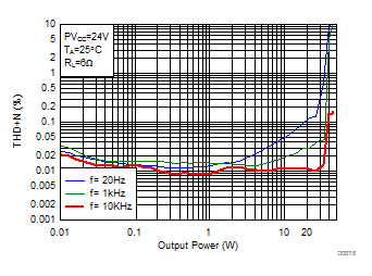
1.
Figure 15. THD+N vs Output Power-BTL | PVDD = 24 V | 1SPW Modulation | 10 µH + 0.68 µF |
| FSW = 768 kHz | Load = 6 Ω |
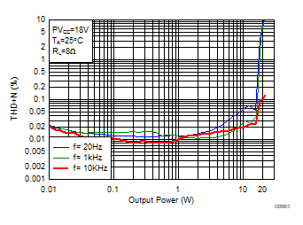
1.
Figure 17. THD+N vs Output Power-BTL | PVDD = 18 V | 1SPW Modulation | 10 µH + 0.68 µF |
| FSW = 768 kHz | Load = 8 Ω |
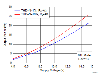
1. Dashed lines represent thermally limited region for the continuous output power.
Figure 19. Output Power vs Supply Voltage | PVDD = 4.5V~16V | 1SPW Modulation | 4.7 µH + 0.68 µF |
| FSW = 768 kHz | Load = 4 Ω |
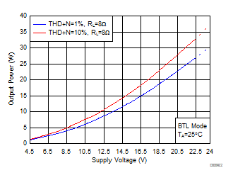
1. Dashed lines represent thermally limited region for the continuous output power.
Figure 21. Output Power vs Supply Voltage | PVDD = 4.5V~24V | 1SPW Modulation | 10 µH + 0.68 µF |
| FSW = 768 kHz | Load = 8 Ω |
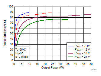
1.
Figure 23. Efficiency vs Supply Voltage | PVDD = 7.4 V, 12 V, 18 V, 24 V | 10 µH + 0.68 µF | |
| FSW = 768 kHz | Load = 6 Ω | 1 SPW Modulation |
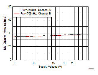
1.
Figure 25. Idle Channel Noise vs Supply Voltage | PVDD = 4.5V~24V | 1 SPW Modulation | 10 µH + 0.68 µF |
| FSW = 768 kHz | Load = 8 Ω |
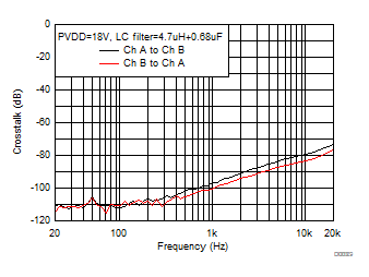
1.
Figure 27. Crosstalk | PVDD = 18 V | 1 SPW Modulation | 10 µH + 0.68 µF |
| FSW = 768 kHz | Load = 6 Ω | PO = 1 W |

1.
Figure 29. Crosstalk | PVDD = 12 V | 1 SPW Modulation | 4.7 µH + 0.68 µF |
| FSW = 768 kHz | Load = 8 Ω | PO = 1 W |

1.
Figure 31. Crosstalk | PVDD = 24 V | 1 SPW Modulation | 10 µH + 0.68 µF |
| FSW = 768 kHz | Load = 8 Ω | PO = 1 W |
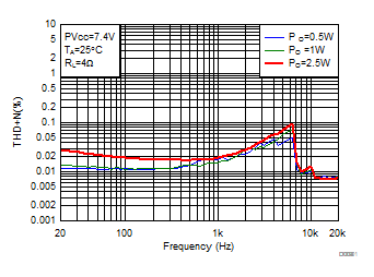
| PVDD = 7.4 V | 4.7 µH + 0.68 µF | |
| FSW = 576 kHz | 1SPW Modulation | Load = 4 Ω |
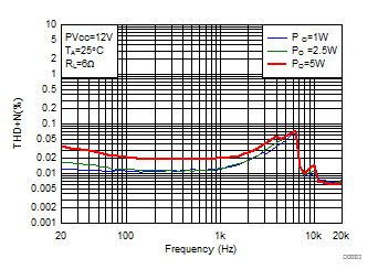
| PVDD = 12 V | 4.7 µH + 0.68 µF | |
| FSW = 768 kHz | 1SPW Modulation | Load = 6 Ω |
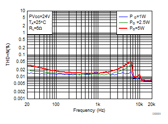
| PVDD = 24 V | 10 µH + 0.68 µF | |
| FSW = 768 kHz | 1SPW Modulation | Load = 6 Ω |
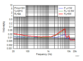
| PVDD = 18 V | 10 µH + 0.68 µF | |
| FSW = 768 kHz | 1SPW Modulation | Load = 8 Ω |
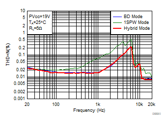
1.
Figure 10. THD+N vs Frequency-BTL | PVDD = 19 V | Hybrid, BD | PO = 5 W |
| FSW = 384 kHz | 1 SPW Modulation | Load = 6 Ω |
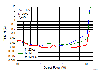
1.
Figure 12. THD+N vs Output Power-BTL | PVDD = 12 V | 1SPW Modulation | 4.7 µH + 0.68 µF |
| FSW = 768 kHz | Load = 4 Ω |
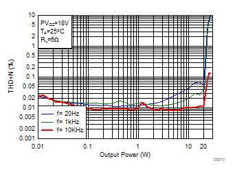
1.
Figure 14. THD+N vs Output Power-BTL | PVDD = 18 V | 1SPW Modulation | 10 µH + 0.68 µF |
| FSW = 768 kHz | Load = 6 Ω |
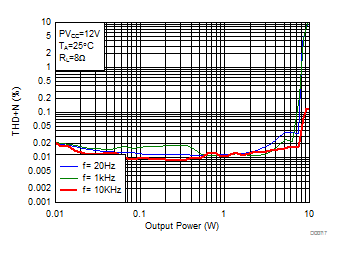
1.
Figure 16. THD+N vs Output Power-BTL | PVDD = 12 V | 1SPW Modulation | 10 µH + 0.68 µF |
| FSW = 768 kHz | Load = 8 Ω |
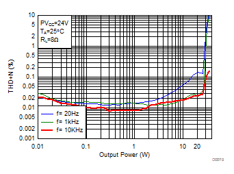
1.
Figure 18. THD+N vs Output Power-BTL | PVDD = 24 V | 1SPW Modulation | 10 µH + 0.68 µF |
| FSW = 768 kHz | Load = 8 Ω |
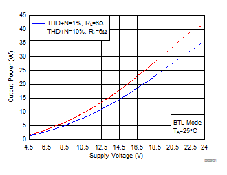
1. Dashed lines represent thermally limited region for the continuous output power.
Figure 20. Output Power vs Supply Voltage | PVDD = 4.5V~24V | 1SPW Modulation | 10 µH + 0.68 µF |
| FSW = 768 kHz | Load = 6 Ω |
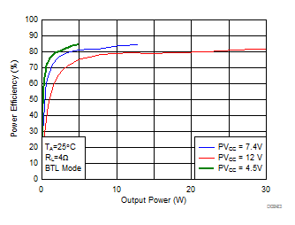
1.
Figure 22. Efficiency vs Supply Voltage | PVDD = 4.5 V, 7.4 V, 12 V | 1 SPW Modulation | |
| FSW = 768 kHz | Load = 4 Ω | 4.7 µH + 0.68 µF |
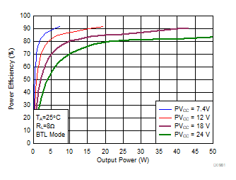
1.
Figure 24. Efficiency vs Supply Voltage | PVDD = 7.4 V, 12 V, 18 V, 24 V | 10 µH + 0.68 µF | |
| FSW = 768 kHz | Load = 8 Ω | 1SPW Modulation |
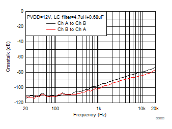
1.
Figure 26. Crosstalk | PVDD = 12 V | 1 SPW Modulation | 4.7 µH + 0.68 µF |
| FSW = 768 kHz | Load = 6 Ω | PO = 1 W |
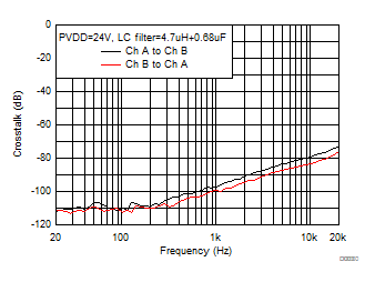
1.
Figure 28. Crosstalk | PVDD = 24 V | 1 SPW Modulation | 10 µH + 0.68 µF |
| FSW = 768 kHz | Load = 6 Ω | PO = 1 W |

1.
Figure 30. Crosstalk | PVDD = 18 V | 1 SPW Modulation | 10 µH + 0.68 µF |
| FSW = 768 kHz | Load = 8 Ω | PO = 1 W |