JAJSHH5 May 2019 TAS5806MD
PRODUCTION DATA.
- 1 特長
- 2 アプリケーション
- 3 概要
- 4 改訂履歴
- 5 概要(続き)
- 6 Device Comparison Table
- 7 Pin Configuration and Functions
- 8 Specifications
- 9 Parametric Measurement Information
-
10Detailed Description
- 10.1 Overview
- 10.2 Functional Block Diagram
- 10.3 Feature Description
- 10.4 Device Functional Modes
- 10.5 Programming and Control
- 10.6
Register Maps
- 10.6.1
CONTROL PORT Registers
- 10.6.1.1 RESET_CTRL Register (Offset = 1h) [reset = 0x00]
- 10.6.1.2 DEVICE_CTRL_1 Register (Offset = 2h) [reset = 0x00]
- 10.6.1.3 DEVICE_CTRL_2 Register (Offset = 3h) [reset = 0x10]
- 10.6.1.4 I2C_PAGE_AUTO_INC Register (Offset = Fh) [reset = 0x00]
- 10.6.1.5 SIG_CH_CTRL Register (Offset = 28h) [reset = 0x00]
- 10.6.1.6 CLOCK_DET_CTRL Register (Offset = 29h) [reset = 0x00]
- 10.6.1.7 SDOUT_SEL Register (Offset = 30h) [reset = 0h]
- 10.6.1.8 I2S_CTRL Register (Offset = 31h) [reset = 0x00]
- 10.6.1.9 SAP_CTRL1 Register (Offset = 33h) [reset = 0x02]
- 10.6.1.10 SAP_CTRL2 Register (Offset = 34h) [reset = 0x00]
- 10.6.1.11 SAP_CTRL3 Register (Offset = 35h) [reset = 0x11]
- 10.6.1.12 FS_MON Register (Offset = 37h) [reset = 0x00]
- 10.6.1.13 BCK_MON Register (Offset = 38h) [reset = 0x00]
- 10.6.1.14 CLKDET_STATUS Register (Offset = 39h) [reset = 0x00]
- 10.6.1.15 CHANNEL_FORCE_HIZ Register (Offset = 40h) [reset = 0x01]
- 10.6.1.16 DIG_VOL_CTL Register (Offset = 4Ch) [reset = 30h]
- 10.6.1.17 DIG_VOL_CTRL2 Register (Offset = 4Eh) [reset = 0x33]
- 10.6.1.18 DIG_VOL_CTRL3 Register (Offset = 4Fh) [reset = 0x30]
- 10.6.1.19 AUTO_MUTE_CTRL Register (Offset = 50h) [reset = 0x07]
- 10.6.1.20 AUTO_MUTE_TIME Register (Offset = 51h) [reset = 0x00]
- 10.6.1.21 ANA_CTRL Register (Offset = 53h) [reset = 0x00]
- 10.6.1.22 AGAIN Register (Offset = 54h) [reset = 0x00]
- 10.6.1.23 BQ_WR_CTRL1 Register (Offset = 5Ch) [reset = 0x00]
- 10.6.1.24 DAC_CTRL Register (Offset = 5Dh) [reset = 0xF8]
- 10.6.1.25 ADR_PIN_CTRL Register (Offset = 60h) [reset = 0h]
- 10.6.1.26 ADR_PIN_CONFIG Register (Offset = 61h) [reset = 0x00]
- 10.6.1.27 DSP_MISC Register (Offset = 66h) [reset = 0h]
- 10.6.1.28 DIE_ID Register (Offset = 67h) [reset = 0h]
- 10.6.1.29 POWER_STATE Register (Offset = 68h) [reset = 0x00]
- 10.6.1.30 AUTOMUTE_STATE Register (Offset = 69h) [reset = 0x00]
- 10.6.1.31 PHASE_CTRL Register (Offset = 6Ah) [reset = 0x00]
- 10.6.1.32 SS_CTRL0 Register (Offset = 6Bh) [reset = 0x00]
- 10.6.1.33 SS_CTRL1 Register (Offset = 6Ch) [reset = 0x00]
- 10.6.1.34 SS_CTRL2 Register (Offset = 6Dh) [reset = 0x50]
- 10.6.1.35 SS_CTRL3 Register (Offset = 6Eh) [reset = 0x11]
- 10.6.1.36 SS_CTRL4 Register (Offset = 6Fh) [reset = 0x24]
- 10.6.1.37 CHAN_FAULT Register (Offset = 70h) [reset = 0x00]
- 10.6.1.38 GLOBAL_FAULT1 Register (Offset = 71h) [reset = 0h]
- 10.6.1.39 GLOBAL_FAULT2 Register (Offset = 72h) [reset = 0h]
- 10.6.1.40 OT WARNING Register (Offset = 73h) [reset = 0x00]
- 10.6.1.41 PIN_CONTROL1 Register (Offset = 74h) [reset = 0x00]
- 10.6.1.42 PIN_CONTROL2 Register (Offset = 75h) [reset = 0xF8]
- 10.6.1.43 MISC_CONTROL Register (Offset = 76h) [reset = 0x00]
- 10.6.1.44 HP_CONTROL Register (Offset = 77h) [reset = 0x00]
- 10.6.1.45 FAULT_CLEAR Register (Offset = 78h) [reset = 0x00]
- 10.6.1
CONTROL PORT Registers
- 11Application and Implementation
- 12Power Supply Recommendations
- 13Layout
- 14デバイスおよびドキュメントのサポート
- 15メカニカル、パッケージ、および注文情報
パッケージ・オプション
メカニカル・データ(パッケージ|ピン)
- DCP|38
サーマルパッド・メカニカル・データ
- DCP|38
発注情報
10.3.8.1 Speaker Amplifier Gain Select
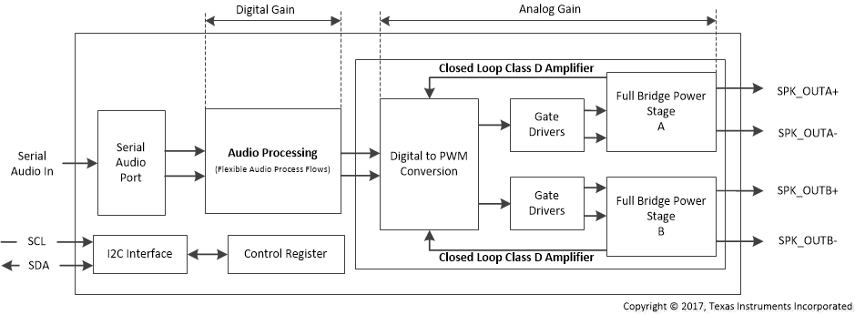
A combination of digital gain and analog gain is used to provide the overall gain of the speaker amplifier. As seen in Figure 72, the audio path of the TAS5806MD consists of a digital audio input port, a digital audio path, a digital to PWM converter (DPC), a gate driver stage, a Class D power stage, and a feedback loop which feeds the output information back into the DPC block to correct for distortion sensed on the output pins. The total amplifier gain is comprised of digital gain, shown in the digital audio path and the analog gain from the input of the analog modulator to the output of the speaker amplifier power stage.
 Figure 72. Speaker Amplifier Gain
 As shown in Figure 72, the first gain stage for the speaker amplifier is present in the digital audio path. It consists of the volume control and the digital boost block. The volume control is set to 0dB by default, it does not change. For all settings of the register 0x54, AGAIN[4:0], the digital boost block remains at 0 dB. These gain settings ensure that the output signal is not clipping at different PVDD levels. 0dBFS output is 29.5-V peak output voltage
Table 2. Analog Gain Setting
| AGAIN <4:0> | GAIN (dBFS) | AMPLIFIER OUTPUT PEAK VOLTAGE (V) |
|---|---|---|
| 00000 | 0 | 29.5 |
| 00001 | -0.5 | 27.85 |
| ……. | …….. | ……. |
| 11111 | -15.5 | 4.95 |