JAJSM14B June 2021 – October 2023 TCA39306-Q1
PRODUCTION DATA
- 1
- 1 特長
- 2 アプリケーション
- 3 概要
- 4 Pin Configuration and Functions
- 5 Specifications
- 6 Parameter Measurement Information
-
7 Detailed Description
- 7.1
Overview
- 7.1.1 Definition of threshold voltage
- 7.1.2 Correct Device Set Up
- 7.1.3 Disconnecting a Target from the Main Bus Using the EN Pin
- 7.1.4 Supporting Remote Board Insertion to Backplane with TCA39306-Q1
- 7.1.5 Switch Configuration
- 7.1.6 Controller on Side 1 or Side 2 of Device
- 7.1.7 LDO and TCA39306-Q1 Concerns
- 7.1.8 Current Limiting Resistance on VREF2
- 7.2 Functional Block Diagram
- 7.3 Feature Description
- 7.4 Device Functional Modes
- 7.1
Overview
- 8 Application and Implementation
- 9 Device and Documentation Support
- 10Revision History
- 11Mechanical, Packaging, and Orderable Information
7.1.5 Switch Configuration
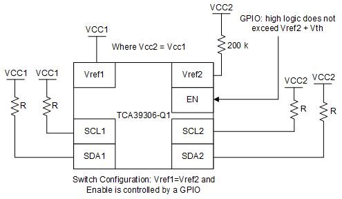
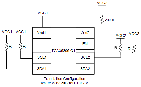
TCA39306-Q1 has the capability of being used with its VREF1 voltage equal to VREF2. This essentially turns the device from a translator to a device which can be used as a switch, and in some situations this can be useful. The switch configuration is shown in Figure 7-5 and translation mode is shown in Figure 7-6.
 Figure 7-5 Switch
Configuration
 Figure 7-6 Translation Configuration
When TCA39306-Q1 is in the switch configuration (VREF1 = VREF2), the propagation delays are different compared to the translator configuration. Taking a look at the propagation delays, if the pull up resistance and capacitance on both sides of the bus are equal, then in switch mode the device has the same propagation delay from side one to two and side two to one. The propagation delays become lower when VCC1/VCC2 is larger. For example, the propagation delay at 1.8 V is longer than at 5 V in the switching configuration. When the device is in translation mode, side one propagate lows to side two faster than side two can propagate lows to side 1. This time difference becomes larger the larger the difference between VCC2 and VCC1 becomes.