SCPS164D MAY 2007 – February 2017 TCA6507
PRODUCTION DATA.
- 1 Features
- 2 Applications
- 3 Description
- 4 Revision History
- 5 Pin Configuration and Functions
- 6 Specifications
- 7 Parameter Measurement Information
-
8 Detailed Description
- 8.1 Overview
- 8.2 Functional Block Diagram
- 8.3 Feature Description
- 8.4 Device Functional Modes
- 8.5 Programming
- 8.6
Register Maps
- 8.6.1 Registers 0x00 - 0x02 (Select Registers)
- 8.6.2 Register 0x03 (Fade-ON Time)
- 8.6.3 Register 0x04 (Fully-ON Time)
- 8.6.4 Register 0x05 (Fade-OFF Time)
- 8.6.5 Register 0x06 - 0x07 (Fully-OFF Time)
- 8.6.6 Register 0x08 (Maximum Intensity per Bank)
- 8.6.7 Register 0x09 (One-Shot / Master Intensity)
- 8.6.8 Register 0x0A (Initialization Register)
- 9 Application and Implementation
- 10Power Supply Recommendations
- 11Layout
- 12Device and Documentation Support
- 13Mechanical, Packaging, and Orderable Information
パッケージ・オプション
メカニカル・データ(パッケージ|ピン)
サーマルパッド・メカニカル・データ
- RUE|12
発注情報
7 Parameter Measurement Information

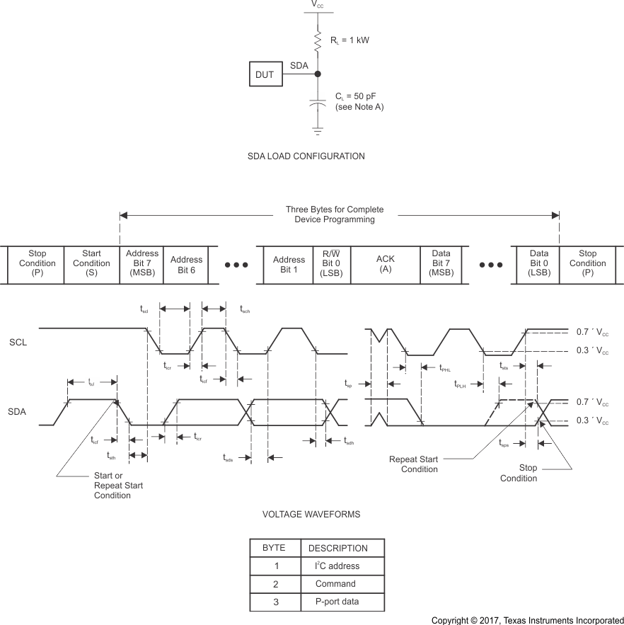
A. CL includes probe and jig capacitance.
B. All inputs are supplied by generators having the following characteristics: PRR ≤ 10 MHz, ZO = 50 Ω, tr/tf ≤ 30 ns.
C. All parameters and waveforms are not applicable to all devices.
Figure 8. I2C Interface Load Circuit and Voltage Waveforms

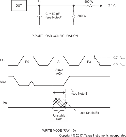
A. CL includes probe and jig capacitance.
B. All inputs are supplied by generators having the following characteristics: PRR ≤ 10 MHz, ZO = 50 Ω, tr/tf ≤ 30 ns.
C. The outputs are measured one at a time, with one transition per measurement.
D. All parameters and waveforms are not applicable to all devices.
Figure 9. P-Port Load Circuit and Voltage Waveforms