SCPS222C May 2010 – October 2015 TCA8418E
PRODUCTION DATA.
- 1 Features
- 2 Applications
- 3 Description
- 4 Revision History
- 5 Pin Configuration and Functions
-
6 Specifications
- 6.1 Absolute Maximum Ratings
- 6.2 ESD Ratings
- 6.3 Recommended Operating Conditions
- 6.4 Thermal Information
- 6.5 Electrical Characteristics
- 6.6 I2C Interface Timing Requirements
- 6.7 Reset Timing Requirements for Standard Mode, Fast Mode, Fast Mode Plus (FM+) I2C Bus
- 6.8 Switching Characteristics for Standard Mode, Fast Mode, Fast Mode Plus (FM+) I2C Bus
- 6.9 Keypad Switching Characteristics for Standard Mode, Fast Mode, Fast Mode Plus (FM+) I2C Bus
- 6.10 Typical Characteristics
- 7 Parameter Measurement Information
-
8 Detailed Description
- 8.1 Overview
- 8.2 Functional Block Diagram
- 8.3 Feature Description
- 8.4 Device Functional Modes
- 8.5 Programming
- 8.6
Register Maps
- 8.6.1 Device Address
- 8.6.2
Control Register and Command Byte
- 8.6.2.1 Configuration Register (Address 0x01)
- 8.6.2.2 Interrupt Status Register, INT_STAT (Address 0x02)
- 8.6.2.3 Key Lock and Event Counter Register, KEY_LCK_EC (Address 0x03)
- 8.6.2.4 Key Event Registers (FIFO), KEY_EVENT_A-J (Address 0x04-0x0D)
- 8.6.2.5 Keypad Lock1 to Lock2 Timer Register, KP_LCK_TIMER (Address 0x0E)
- 8.6.2.6 Unlock1 and Unlock2 Registers, UNLOCK1/2 (Address 0x0F-0x10)
- 8.6.2.7 GPIO Interrupt Status Registers, GPIO_INT_STAT1-3 (Address 0x11-0x13)
- 8.6.2.8 GPIO Data Status Registers, GPIO_DAT_STAT1-3 (Address 0x14-0x16)
- 8.6.2.9 GPIO Data Out Registers, GPIO_DAT_OUT1-3 (Address 0x17-0x19)
- 8.6.2.10 GPIO Interrupt Enable Registers, GPIO_INT_EN1-3 (Address 0x1A-0x1C)
- 8.6.2.11 Keypad or GPIO Selection Registers, KP_GPIO1-3 (Address 0x1D-0x1F)
- 8.6.2.12 GPI Event Mode Registers, GPI_EM1-3 (Address 0x20-0x22)
- 8.6.2.13 GPIO Data Direction Registers, GPIO_DIR1-3 (Address 0x23-0x25)
- 8.6.2.14 GPIO Edge/Level Detect Registers, GPIO_INT_LVL1-3 (Address 0x26-0x28)
- 8.6.2.15 Debounce Disable Registers, DEBOUNCE_DIS1-3 (Address 0x29-0x2B)
- 8.6.2.16 GPIO Pullup Disable Register, GPIO_PULL1-3 (Address 0x2C-0x2E)
- 9 Application and Implementation
- 10Power Supply Recommendations
- 11Layout
- 12Device and Documentation Support
- 13Mechanical, Packaging, and Orderable Information
6 Specifications
6.1 Absolute Maximum Ratings(1)
over operating free-air temperature range (unless otherwise noted)| MIN | MAX | UNIT | ||||
|---|---|---|---|---|---|---|
| VCC | Supply voltage | –0.5 | 4.6 | V | ||
| VI | Input voltage (2) | –0.5 | 4.6 | V | ||
| VO | Voltage range applied to any output in the high-impedance or power-off state(2) | –0.5 | 4.6 | V | ||
| Output voltage in the high or low state(2) | –0.5 | 4.6 | ||||
| IIK | Input clamp current | VI < 0 | ±20 | mA | ||
| IOK | Output clamp current | VO < 0 | ±20 | mA | ||
| IOL | Continuous output Low current | P port, SDA | VO = 0 to VCC | 50 | mA | |
| INT | 25 | |||||
| IOH | Continuous output High current | P port | VO = 0 to VCC | 50 | ||
| Tstg | Storage temperature | –65 | 150 | °C | ||
(1) Stresses beyond those listed under Absolute Maximum Ratings may cause permanent damage to the device. These are stress ratings only, and functional operation of the device at these or any other conditions beyond those indicated under Recommended Operating Conditions is not implied. Exposure to absolute-maximum-rated conditions for extended periods may affect device reliability.
(2) The input negative-voltage and output voltage ratings may be exceeded if the input and output current ratings are observed.
6.2 ESD Ratings
| VALUE | UNIT | ||||
|---|---|---|---|---|---|
| V(ESD) | Electrostatic discharge | Human-body model (HBM), per ANSI/ESDA/JEDEC JS-001 (Non-GPIO pins)(1) | ±2000 | V | |
| Charged-device model (CDM), per JEDEC specification JESD22-C101(2) | ±1000 | ||||
| Human-body model (HBM), per ANSI/ESDA/JEDEC JS-001 (GPIO pins)(1) | ±15000 | ||||
(1) JEDEC document JEP155 states that 500-V HBM allows safe manufacturing with a standard ESD control process.
(2) JEDEC document JEP157 states that 250-V CDM allows safe manufacturing with a standard ESD control process.
6.3 Recommended Operating Conditions
| MIN | MAX | UNIT | |||
|---|---|---|---|---|---|
| VCC | Supply voltage | 1.65 | 3.6 | V | |
| VIH | High-level input voltage | SCL, SDA, ROW0–7, COL0–9, RESET | 0.7 × VCC | 3.6 | V |
| VIL | Low-level input voltage | SCL, SDA, ROW0–7, COL0–9, RESET | –0.5 | 0.3 × VCC | V |
| IOH | High-level output current | ROW0–7, COL0–9 | 10 | mA | |
| IOL | Low-level output current | ROW0–7, COL0–9 | 25 | mA | |
| TA | Operating free-air temperature | –40 | 85 | °C | |
6.4 Thermal Information
over operating free-air temperature range (unless otherwise noted)| THERMAL METRIC(1) | TCA8418E | UNIT | |
|---|---|---|---|
| YFP (DSBGA) | |||
| 25 PINS | |||
| RθJA | Junction-to-ambient thermal resistance | 61.2 | °C/W |
| RθJC(top) | Junction-to-case (top) thermal resistance | 0.4 | °C/W |
| RθJB | Junction-to-board thermal resistance | 10.6 | °C/W |
| ψJT | Junction-to-top characterization parameter | 1.0 | °C/W |
| ψJB | Junction-to-board characterization parameter | 10.6 | °C/W |
| RθJC(bot) | Junction-to-case (bottom) thermal resistance | N/A | °C/W |
(1) For more information about traditional and new thermal metrics, see the Semiconductor and IC Package Thermal Metrics application report, SPRA953.
6.5 Electrical Characteristics
over recommended operating free-air temperature range, VCC = 1.65 V to 3.6 V (unless otherwise noted)| PARAMETER | TEST CONDITIONS | VCC | MIN | TYP | MAX | UNIT | |||
|---|---|---|---|---|---|---|---|---|---|
| VIK | Input diode clamp voltage | II = –18 mA | 1.65 V to 3.6 V | –1.2 | V | ||||
| VPORR | Power-on reset voltage, VCC rising | VI = VCCP or GND, IO = 0 | 1.65 V to 3.6 V | 1.03 | 1.43 | V | |||
| VPORF | Power-on reset voltage, VCC falling | 0.76 | 1.15 | ||||||
| VOH | ROW0–7, COL0–9 high-level output voltage | IOH = –1 mA | 1.65 V | 1.25 | V | ||||
| IOH = –8 mA | 1.65 V | 1.2 | |||||||
| 2.3 V | 1.8 | ||||||||
| 3 V | 2.6 | ||||||||
| IOH = –10 mA | 1.65 V | 1.1 | |||||||
| 2.3 V | 1.7 | ||||||||
| 3 V | 2.5 | ||||||||
| VOL | ROW0–7, COL0–9 low-level output voltage | IOL = 1 mA | 1.65 V | 0.4 | V | ||||
| IOL = 8 mA | 1.65 V | 0.45 | |||||||
| 2.3 V | 0.25 | ||||||||
| 3 V | 0.25 | ||||||||
| IOL = 10 mA | 1.65 V | 0.6 | |||||||
| 2.3 V | 0.3 | ||||||||
| 3 V | 0.25 | ||||||||
| IOL | SDA | VOL = 0.4 V | 1.65 V to 3.6 V | 3 | mA | ||||
| INT and CAD_INT | VOL = 0.4 V | 1.65 V to 3.6 V | 3 | ||||||
| II | SCL, SDA, ROW0–7, COL0–9, RESET | VI = VCCI or GND | 1.65 V to 3.6 V | 1 | μA | ||||
| RINT | Internal pullup resistor value | ROW0–7, COL0–9 | 55 | kΩ | |||||
| ICC Supply Voltage | VI on SDA, ROW0–7, COL0–9 = VCC or GND, IO = 0, I/O = inputs, |
fSCL = 0 kHz | Oscillator OFF | 1.65 V to 3.6 V | 13 | μA | |||
| Oscillator ON | 18 | ||||||||
| fSCL = 400 kHz | 1 key press | 1.65 V | 15 | ||||||
| 3.6 V | 30 | ||||||||
| fSCL = 1 MHz | 1.65 V | 15 | |||||||
| 3.6 V | 40 | ||||||||
| fSCL = 400 kHz | GPI low (pullup enable)(1) | 1.65 V to 3.6 V | 115 | ||||||
| fSCL = 1 MHz | 125 | ||||||||
| fSCL = 400 kHz | GPI low (pullup disable) | 25 | |||||||
| fSCL = 1 MHz | 35 | ||||||||
| fSCL = 400 kHz | 1 GPO active | 115 | |||||||
| fSCL = 1 MHz | 125 | ||||||||
| CI | SCL | VI = VCC or GND | 1.65 V to 3.6 V | 6 | 8 | pF | |||
| Cio | SDA | VIO = VCC or GND | 1.65 V to 3.6 V | 10 | 12.5 | pF | |||
| ROW0–7, COL0–9 | 5 | 6 | |||||||
(1) Assumes that one GPIO is enabled.
6.6 I2C Interface Timing Requirements
over recommended operating free-air temperature range (unless otherwise noted) (see Figure 16)| STANDARD MODE I2C BUS |
FAST MODE I2C BUS |
FAST MODE PLUS (FM+) I2C BUS |
UNIT | |||||
|---|---|---|---|---|---|---|---|---|
| MIN | MAX | MIN | MAX | MIN | MAX | |||
| fscl | I2C clock frequency | 0 | 100 | 0 | 400 | 0 | 1000 | kHz |
| tsch | I2C clock high time | 4 | 0.6 | 0.26 | μs | |||
| tscl | I2C clock low time | 4.7 | 1.3 | 0.5 | μs | |||
| tsp | I2C spike time | 50 | 50 | 50 | ns | |||
| tsds | I2C serial data setup time | 250 | 100 | 50 | ns | |||
| tsdh | I2C serial data hold time | 0 | 0 | 0 | ns | |||
| ticr | I2C input rise time | 1000 | 20 + 0.1Cb (1) | 300 | 120 | ns | ||
| ticf | I2C input fall time | 300 | 20 + 0.1Cb(1) | 300 | 120 | ns | ||
| tocf | I2C output fall time; 10 pF to 400 pF bus | 300 | 20 + 0.1Cb (1) | 300 | 120 | μs | ||
| tbuf | I2C bus free time between Stop and Start | 4.7 | 1.3 | 0.5 | μs | |||
| tsts | I2C Start or repeater Start condition setup time | 4.7 | 0.6 | 0.26 | μs | |||
| tsth | I2C Start or repeater Start condition hold time | 4 | 0.6 | 0.26 | μs | |||
| tsps | I2C Stop condition setup time | 4 | 0.6 | 0.26 | μs | |||
| tvd(data) | Valid data time; SCL low to SDA output valid | 1 | 0.9 | 0.45 | μs | |||
| tvd(ack) | Valid data time of ACK condition; ACK signal from SCL low to SDA (out) low | 1 | 0.9 | 0.45 | μs | |||
(1) Cb = total capacitance of one bus line in pF
6.7 Reset Timing Requirements for Standard Mode, Fast Mode, Fast Mode Plus (FM+) I2C Bus
over recommended operating free-air temperature range (unless otherwise noted) (see Figure 19)| MIN | MAX | UNIT | ||
|---|---|---|---|---|
| tW | Reset pulse duration | 120(1) | μs | |
| tREC | Reset recovery time | 120(1) | μs | |
| tRESET | Time to reset | 120(1) | μs | |
(1) The GPIO debounce circuit uses each GPIO input which passes through a two-stage register circuit. Both registers are clocked by the same clock signal, presumably free-running, with a nominal period of 50 μs. When an input changes state, the new state is clocked into the first stage on one clock transition. On the next same-direction transition, if the input state is still the same as the previously clocked state, the signal is clocked into the second stage, and then on to the remaining circuits. Since the inputs are asynchronous to the clock, it will take anywhere from zero to 50 μs after the input transition to clock the signal into the first stage. Therefore, the total debounce time may be as long as 100 μs. Finally, to account for a slow clock, the spec further guard-banded at 120 μs.
6.8 Switching Characteristics for Standard Mode, Fast Mode, Fast Mode Plus (FM+) I2C Bus
| PARAMETER | FROM | TO | MIN | MAX | UNIT | ||
|---|---|---|---|---|---|---|---|
| tIV | Interrupt valid time | Key event or Key unlock or Overflow | ROW0–7, COL0–9 |
INT | 20 | 60 | μs |
| GPI_INT with Debounce_DIS_Low | 40 | 120 | |||||
| GPI_INT with Debounce_DIS_High | 10 | 30 | |||||
| CAD_INT | INT, CAD_INT | 20 | 60 | ||||
| tIR | Interrupt reset delay time | SCL | INT | 200 | ns | ||
| SCL | CAD_INT | ||||||
| tPV | Output data valid | SCL | ROW0–7, COL0–9 |
400 | ns | ||
| tPS | Input data setup time | P port | SCL | 0 | ns | ||
| tPH | Input data hold time | P port | SCL | 300 | ns | ||
6.9 Keypad Switching Characteristics for Standard Mode, Fast Mode, Fast Mode Plus (FM+) I2C Bus
| PARAMETER | MIN | MAX | UNIT | |
|---|---|---|---|---|
| Key press to detection delay | 25 | μs | ||
| Key release to detection delay | 25 | μs | ||
| Keypad unlock timer | 7 | s | ||
| Keypad interrupt mask timer | 31 | s | ||
| Debounce | 60 | ms | ||
6.10 Typical Characteristics
TA = 25°C (unless otherwise noted)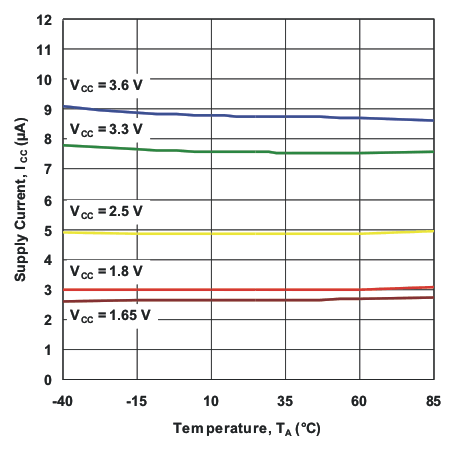 Figure 1. Supply Current vs Temperature
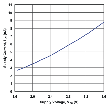 Figure 3. Supply Current vs Supply Voltage
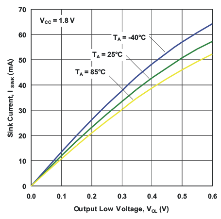 Figure 5. I/O Sink Current vs Output Low Voltage
(VCC = 1.8 V)
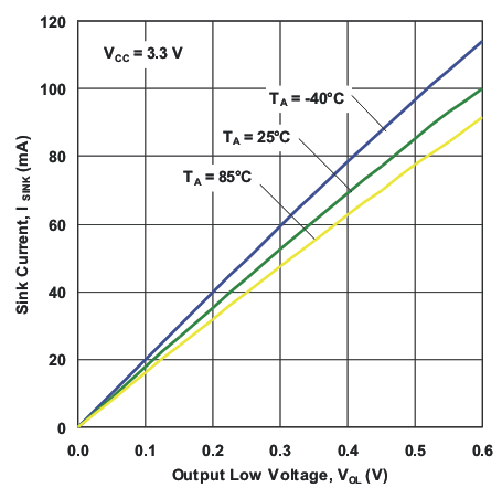 Figure 7. I/O Sink Current vs Output Low Voltage
 (VCC = 3.3 V)
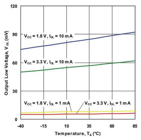 Figure 9. I/O Low Voltage vs Temperature
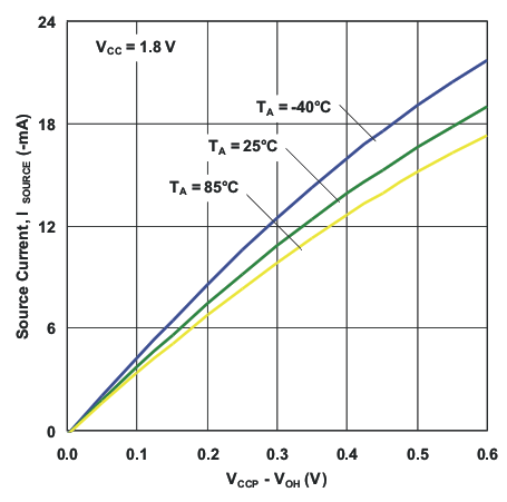 Figure 11. I/O Source Current vs Output High Voltage
 (VCC = 1.8 V)
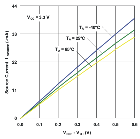 Figure 13. I/O Source Current vs Output High Voltage
 (VCC = 3.3 V)
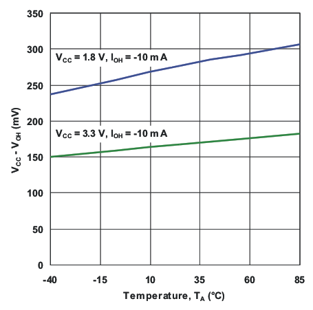 Figure 15. I/O High Voltage vs Temperature
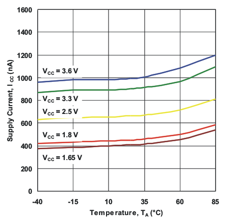 Figure 2. Standby Supply Current vs Temperature
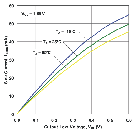 Figure 4. I/O Sink Current vs Output Low Voltage
 (VCC = 1.65 V)
 Figure 6. I/O Sink Current vs Output Low Voltage
 (VCC = 2.5 V)
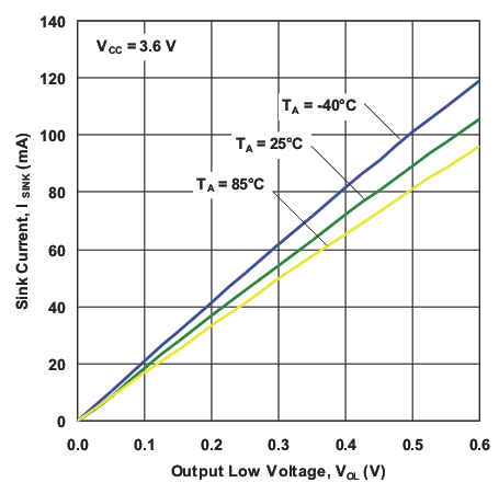 Figure 8. I/O Sink Current vs Output Low Voltage
 (VCC = 3.6 V)
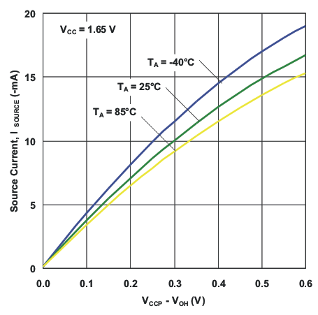 Figure 10. I/O Source Current vs Output High Voltage
 (VCC = 1.65 V)
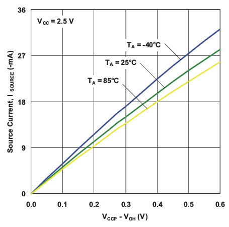 Figure 12. I/O Source Current vs Output High Voltage
 (VCC = 2.5 V)
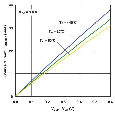 Figure 14. I/O Source Current vs Output High Voltage
 (VCC = 3.6 V)