JAJSHO4D January 2014 – November 2019 TCA9545A
PRODUCTION DATA.
- 1 特長
- 2 アプリケーション
- 3 概要
- 4 改訂履歴
- 5 概要 (続き)
- 6 Pin Configuration and Functions
- 7 Specifications
- 8 Parameter Measurement Information
- 9 Detailed Description
- 10Application and Implementation
- 11Power Supply Recommendations
- 12Layout
- 13デバイスおよびドキュメントのサポート
- 14メカニカル、パッケージ、および注文情報
8 Parameter Measurement Information

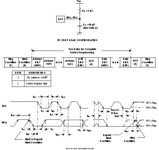
A. CL includes probe and jig capacitance.
B. All input pulses are supplied by generators having the following characteristics: PRR ≤ 10 MHz, ZO = 50 Ω,
tr/tf = 30 ns.
tr/tf = 30 ns.
C. The outputs are measured one at a time, with one transition per measurement.
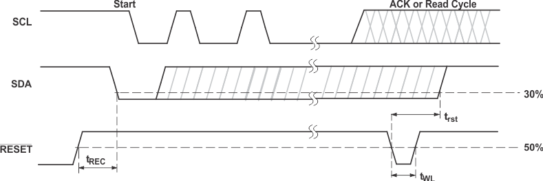
Figure 5. I2C Interface Load Circuit, Byte Descriptions, and Voltage Waveforms  Figure 6. Reset Timing
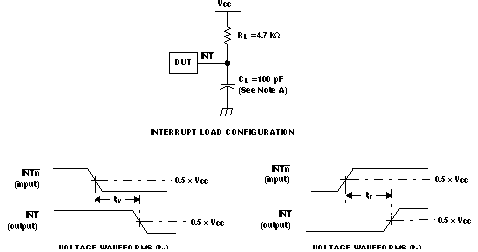
A. CL includes probe and jig capacitance.
B. All input pulses are supplied by generators having the following characteristics: PRR ≤ 10 MHz, ZO = 50 Ω,
tr/tf = 30 ns.
Figure 7. Interrupt Load Circuit and Voltage Waveforms tr/tf = 30 ns.