SCPS196E
December 2010 – February 2017
TCA9554A
PRODUCTION DATA.
1
Features
2
Applications
3
Description
4
Revision History
5
Pin Configuration and Functions
6
Specifications
6.1
Absolute Maximum Ratings
6.2
ESD Ratings
6.3
Recommended Operating Conditions
6.4
Thermal Information
6.5
Electrical Characteristics
6.6
I2C Interface Timing Requirements
6.7
Switching Characteristics
6.8
Typical Characteristics
7
Parameter Measurement Information
8
Detailed Description
8.1
Overview
8.2
Functional Block Diagram
8.3
Feature Description
8.3.1
I/O Port
8.3.2
Interrupt Output (INT)
8.4
Device Functional Modes
8.4.1
Power-On Reset
8.5
Programming
8.5.1
I2C Interface
8.6
Register Maps
8.6.1
Device Address
8.6.2
Control Register and Command Byte
8.6.3
Register Descriptions
8.6.3.1
Bus Transactions
8.6.3.1.1
Writes
8.6.3.1.2
Reads
9
Application and Implementation
9.1
Application Information
9.2
Typical Application
9.2.1
Design Requirements
9.2.1.1
Calculating Junction Temperature and Power Dissipation
9.2.1.2
Minimizing ICC When I/Os Control LEDs
9.2.2
Detailed Design Procedure
9.2.3
Application Curves
10
Power Supply Recommendations
10.1
Power-On Reset Requirements
11
Layout
11.1
Layout Guidelines
11.2
Layout Example
12
Device and Documentation Support
12.1
Documentation Support
12.1.1
Related Documentation
12.2
Receiving Notification of Documentation Updates
12.3
Community Resources
12.4
Trademarks
12.5
Electrostatic Discharge Caution
12.6
Glossary
13
Mechanical, Packaging, and Orderable Information
パッケージ・オプション
メカニカル・データ(パッケージ|ピン)
DW|16
MSOI003I
PW|16
MPDS361A
DBQ|16
MSOI004H
DB|16
MPDS507A
サーマルパッド・メカニカル・データ
DW|16
QFND313D
発注情報
scps196e_oa
scps196e_pm
7
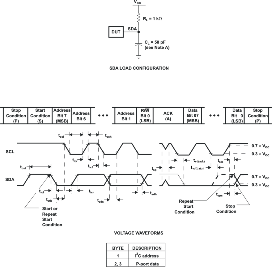
Parameter Measurement Information
A.
C
L
includes probe and jig capacitance.
B.
All inputs are supplied by generators having the following characteristics: PRR ≤ 10 MHz, Z
O
= 50 Ω, t
r
/t
f
≤ 30 ns.
C.
All parameters and waveforms are not applicable to all devices.
Figure 11.
I
2
C Interface Load Circuit and Voltage Waveforms
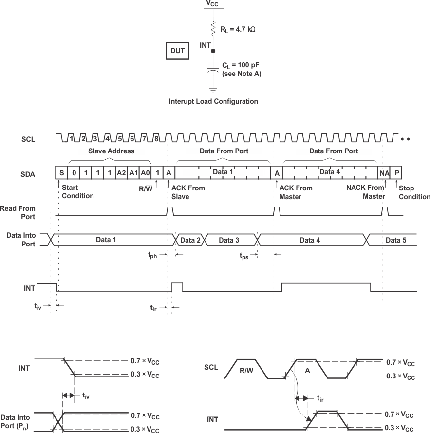
A.
C
L
includes probe and jig capacitance.
B.
All inputs are supplied by generators having the following characteristics: PRR ≤ 10 MHz, Z
O
= 50 Ω, t
r
/t
f
≤ 30 ns.
C.
All parameters and waveforms are not applicable to all devices.
Figure 12.
Interrupt Load Circuit and Voltage Waveforms
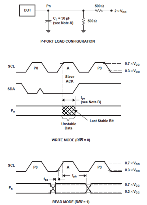
A.
C
L
includes probe and jig capacitance.
B.
t
pv
is measured from 0.7 × V
CC
on SCL to 50% I/O (Pn) output.
C.
All inputs are supplied by generators having the following characteristics: PRR ≤ 10 MHz, Z
O
= 50 Ω, t
r
/t
f
≤ 30 ns.
D.
The outputs are measured one at a time, with one transition per measurement.
E.
All parameters and waveforms are not applicable to all devices.
Figure 13.
P-Port Load Circuit and Voltage Waveforms