JAJSH54E July 2009 – April 2019 TCA9555
PRODUCTION DATA.
- 1 特長
- 2 アプリケーション
- 3 概要
- 4 改訂履歴
- 5 概要(続き)
- 6 Pin Configuration and Functions
- 7 Specifications
- 8 Parameter Measurement Information
- 9 Detailed Description
- 10Application and Implementation
- 11Power Supply Recommendations
- 12Layout
- 13デバイスおよびドキュメントのサポート
- 14メカニカル、パッケージ、および注文情報
パッケージ・オプション
メカニカル・データ(パッケージ|ピン)
サーマルパッド・メカニカル・データ
発注情報
8 Parameter Measurement Information

A. CL includes probe and jig capacitance.
B. All inputs are supplied by generators having the following characteristics: PRR ≤ 10 MHz, ZO = 50 Ω, tr/tf ≤ 30 ns.
C. All parameters and waveforms are not applicable to all devices.
Figure 19. I2C Interface Load Circuit and Voltage Waveforms 
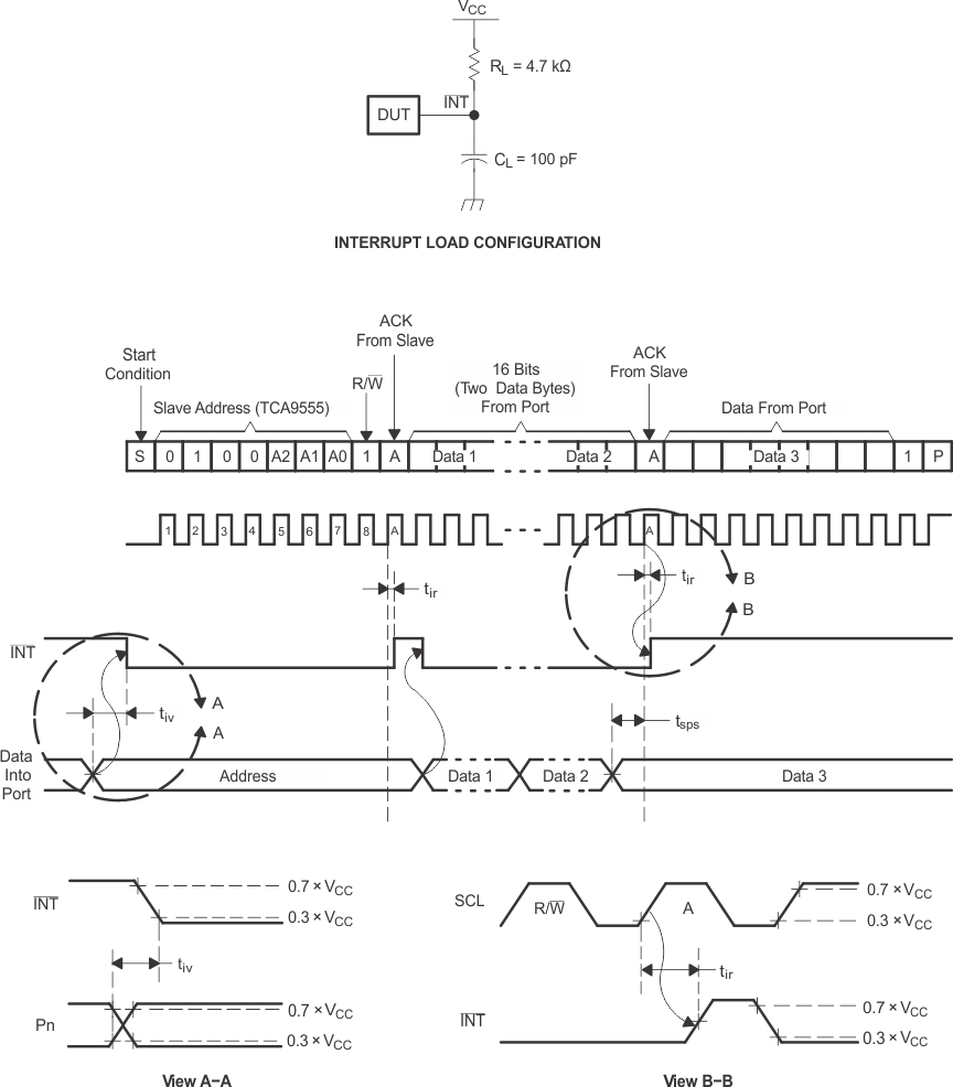
A. CL includes probe and jig capacitance.
B. All inputs are supplied by generators having the following characteristics: PRR ≤ 10 MHz, ZO = 50 Ω, tr/tf ≤ 30 ns.
C. All parameters and waveforms are not applicable to all devices.
Figure 20. Interrupt Load Circuit and Voltage Waveforms 
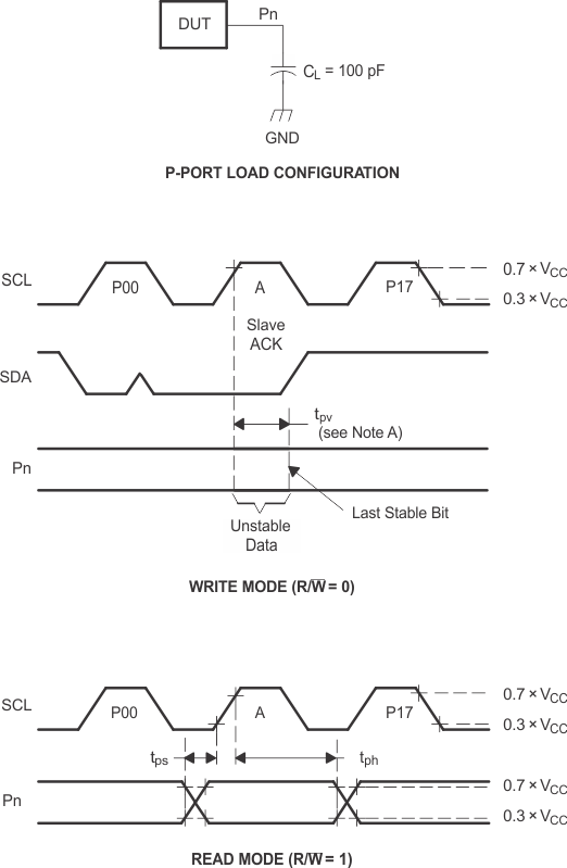
A. CL includes probe and jig capacitance.
B. tpv is measured from 0.7 × VCC on SCL to 50% I/O (Pn) output.
C. All inputs are supplied by generators having the following characteristics: PRR ≤ 10 MHz, ZO = 50 Ω, tr/tf ≤ 30 ns.
D. The outputs are measured one at a time, with one transition per measurement.
E. All parameters and waveforms are not applicable to all devices.
Figure 21. P-Port Load Circuit and Voltage Waveforms