JAJSD11B March   2017  – February 2020 TCA9800

PRODUCTION DATA.  

  1. 特長
  2. アプリケーション
  3. 概要
    1.     Device Images
      1.      概略回路図
  4. 改訂履歴
  5. Device Comparison Table
  6. Pin Configuration and Functions
    1.     Pin Functions
  7. Specifications
    1. 7.1 Absolute Maximum Ratings
    2. 7.2 ESD Ratings
    3. 7.3 Recommended Operating Conditions
    4. 7.4 Thermal Information
    5. 7.5 Electrical Characteristics
    6. 7.6 Timing Requirements
    7. 7.7 Switching Characteristics
    8. 7.8 Typical Characteristics
  8. Parameter Measurement Information
  9. Detailed Description
    1. 9.1 Overview
    2. 9.2 Functional Block Diagram
    3. 9.3 Feature Description
      1. 9.3.1 Integrated Current Source
      2. 9.3.2 Ultra-Low Power Consumption
      3. 9.3.3 No Static-Voltage Offset
      4. 9.3.4 Active-High Repeater Enable Input
      5. 9.3.5 Powered Off High Impedance I2C Bus Pins on A-Side
      6. 9.3.6 Powered-Off Back-Power Protection for I2C Bus Pins
      7. 9.3.7 Clock Stretching and Multiple Master Arbitration Support
    4. 9.4 Device Functional Modes
      1. 9.4.1 Device Operation Considerations
        1. 9.4.1.1 B-Side Input Low (VIL/IILC/RILC)
          1. 9.4.1.1.1 VILC & IILC
          2. 9.4.1.1.2 RILC
        2. 9.4.1.2 Input and Output Leakage Current (IEXT-I/IEXT-O)
          1. 9.4.1.2.1 IEXT-I
          2. 9.4.1.2.2 IEXT-O
  10. 10Application and Implementation
    1. 10.1 Application Information
      1. 10.1.1 Device Selection Guide
      2. 10.1.2 Special Considerations for the B-side
        1. 10.1.2.1 FET or Pass-Gate Translators
        2. 10.1.2.2 Buffered Translators/Level-shifters
    2. 10.2 Typical Application
      1. 10.2.1 Single Device
        1. 10.2.1.1 Design Requirements
        2. 10.2.1.2 Detailed Design Procedure
        3. 10.2.1.3 Application Curves
      2. 10.2.2 Buffering Without Level-Shifting
        1. 10.2.2.1 Design Requirements
        2. 10.2.2.2 Detailed Design Procedure
        3. 10.2.2.3 Application Curve
      3. 10.2.3 Parallel Device Use Case
        1. 10.2.3.1 Design Requirements
        2. 10.2.3.2 Detailed Design Procedure
        3. 10.2.3.3 Application Curves
      4. 10.2.4 Series Device Use Case
        1. 10.2.4.1 Design Requirements
        2. 10.2.4.2 Detailed Design Procedure
        3. 10.2.4.3 Application Curve
  11. 11Power Supply Recommendations
  12. 12Layout
    1. 12.1 Layout Guidelines
    2. 12.2 Layout Example
  13. 13デバイスおよびドキュメントのサポート
    1. 13.1 ドキュメントのサポート
    2. 13.2 ドキュメントの更新通知を受け取る方法
    3. 13.3 サポート・リソース
    4. 13.4 商標
    5. 13.5 静電気放電に関する注意事項
    6. 13.6 Glossary
  14. 14メカニカル、パッケージ、および注文情報

パッケージ・オプション

メカニカル・データ(パッケージ|ピン)
サーマルパッド・メカニカル・データ
発注情報

Buffering Without Level-Shifting

The TCA980x family supports buffering use cases which do not need level-shifting or voltage-translation.

It is critical to note that there are no external sources of current allowed on the B-side ports, since this can affect device operation as shown in the IEXT-I section.
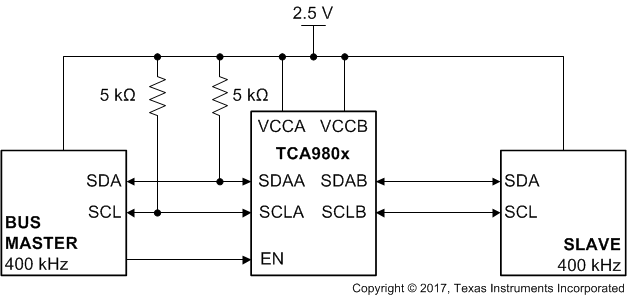
TCA9800 apps_single_buffer.gifFigure 29. Buffering Use Case Without Level-Shifting

NOTE

Decoupling capacitors are not shown to keep the illustration simple. Decoupling capacitors (1 µF and 0.1 µF) must be placed close to each power supply pin.