SCPS290A April 2024 – June 2024 TCAL6416R
PRODUCTION DATA
- 1
- 1 Features
- 2 Applications
- 3 Description
- 4 Pin Configuration and Functions
- 5 Specifications
- 6 Parameter Measurement Information
- 7 Detailed Description
- 8 Application and Implementation
- 9 Device and Documentation Support
- 10Revision History
- 11Mechanical, Packaging, and Orderable Information
パッケージ・オプション
デバイスごとのパッケージ図は、PDF版データシートをご参照ください。
メカニカル・データ(パッケージ|ピン)
- DTO|24
サーマルパッド・メカニカル・データ
発注情報
8.3.1 Power-On Reset Requirements
In the event of a glitch or data corruption, TCAL6416R can be reset to its default conditions by using the power-on reset feature. Power-on reset requires the device go through a power cycle to be completely reset. This reset also happens when the device is powered on for the first time in an application.
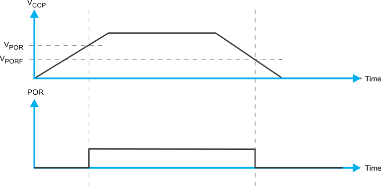
Figure 8-5 and Figure 8-6 shows the two types of power-on reset.
 Figure 8-5 VCCP is Lowered Below 0.2V or 0V and Then Ramped Up
 Figure 8-6 VCCP is Lowered Below the POR Threshold, then Ramped Back Up
Table 8-2 lists the performance of the power-on reset feature for both types of power-on reset.
| PARAMETER(1)(2) | MIN | TYP | MAX | UNIT | ||
|---|---|---|---|---|---|---|
| tFT | Fall rate | See Figure 8-5 | 0.1 | 2000 | ms | |
| tRT | Rise rate | See Figure 8-5 | 0.1 | 2000 | ms | |
| tTRR_GND | Time to re-ramp (when VCC drops to GND) | See Figure 8-5 | 1 | μs | ||
| tTRR_POR50 | Time to re-ramp (when VCC drops to VPOR_MIN – 50mV) | See Figure 8-6 | 1 | μs | ||
| VCC_GH | Level that VCCP can glitch down to, but not cause a functional disruption when VCCP_GW = 1μs | See Figure 8-7 | 1.0 | V | ||
| tGW | Glitch width that will not cause a functional disruption when VCCP_GH = 0.5 × VCCx | See Figure 8-7 | 10 | μs | ||
| VPORF | Voltage trip point of POR on falling VCC | 0.6 | V | |||
| VPORR | Voltage trip point of POR on rising VCC | 1.0 | V | |||
Glitches in the power supply can also affect the power-on reset performance of this device. The glitch width (VCC_GW) and height (VCC_GH) are dependent on each other. The bypass capacitance, source impedance, and device impedance are factors that affect power-on reset performance. For more information on how to measure these specifications, see Figure 8-7 and Table 8-2.
 Figure 8-7 Glitch
Width and Glitch Height
Figure 8-7 Glitch
Width and Glitch HeightVPOR is critical to the power-on reset. VPOR is the voltage level at which the reset condition is released and all the registers and the I2C/SMBus state machine are initialized to their default states. The value of VPOR differs based on the VCCP being lowered to or from 0. For more details on this specification, see Figure 8-8 and Table 8-2.
 Figure 8-8 VPOR