JAJSN07 July 2022 TCAL9539
ADVANCE INFORMATION
- 1 特長
- 2 アプリケーション
- 3 概要
- 4 Revision History
- 5 Pin Configuration and Functions
- 6 Specifications
- 7 Parameter Measurement Information
- 8 Detailed Description
- 9 Application and Implementation
- 10Device and Documentation Support
- 11Mechanical, Packaging, and Orderable Information
パッケージ・オプション
メカニカル・データ(パッケージ|ピン)
サーマルパッド・メカニカル・データ
- RTW|24
発注情報
7 Parameter Measurement Information

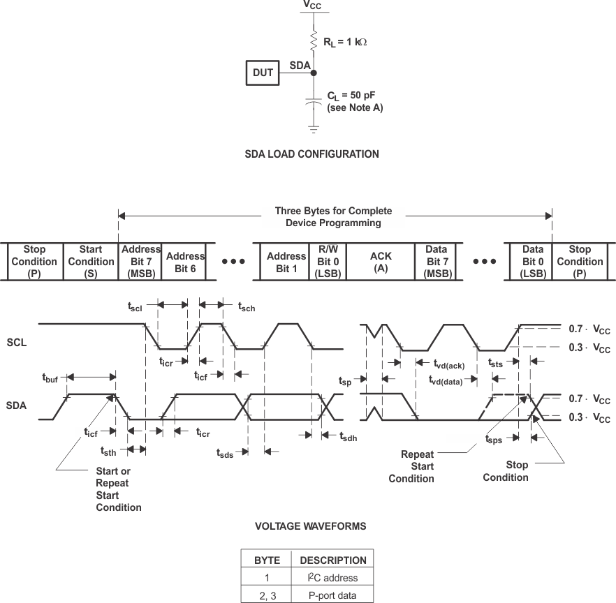
A. CL includes probe and jig capacitance. tocf is measured with
CL of 10 pF or 400 pF.
B. All
inputs are supplied by generators having the following characteristics: PRR ≤ 10
MHz, ZO = 50 Ω, tr/tf ≤ 30 ns.
C. All
parameters and waveforms are not applicable to all devices.
Figure 7-1 I2C Interface Load Circuit and Voltage Waveforms
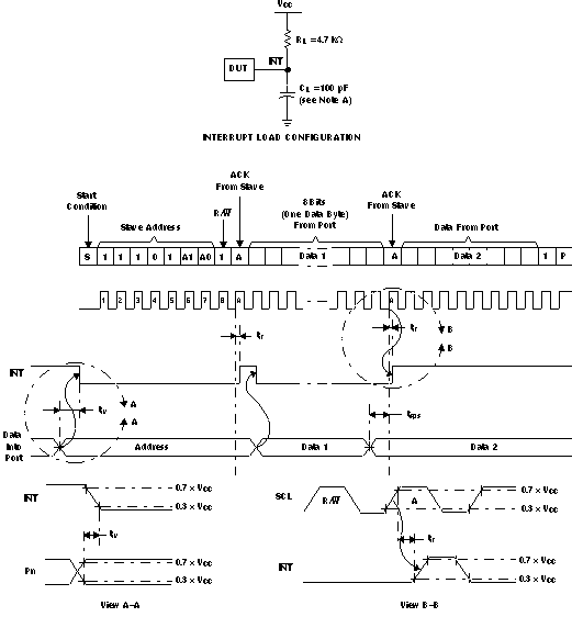
A. CL includes probe and jig capacitance.
B. All
inputs are supplied by generators having the following characteristics: PRR ≤ 10
MHz, ZO = 50 Ω, tr/tf ≤ 30 ns.
C. All
parameters and waveforms are not applicable to all devices.
Figure 7-2 Interrupt
Load Circuit and Voltage Waveforms
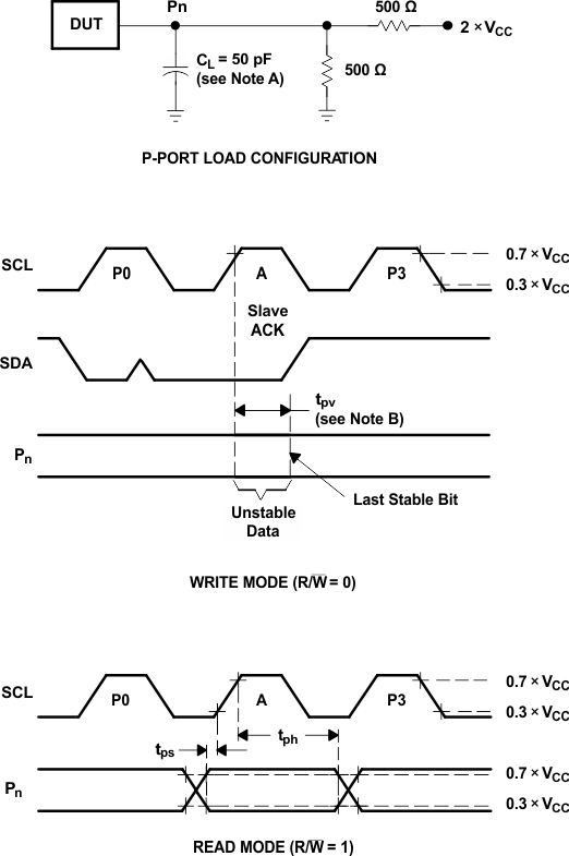
A. CL includes probe and jig capacitance.
B. tpv is measured from 0.7 × VCC on SCL to 50% I/O (Pn)
output.
C. All
inputs are supplied by generators having the following characteristics: PRR ≤ 10
MHz, ZO = 50 Ω, tr/tf ≤ 30 ns.
D. The
outputs are measured one at a time, with one transition per measurement.
E. All
parameters and waveforms are not applicable to all devices.
Figure 7-3 P-Port
Load Circuit and Timing Waveforms
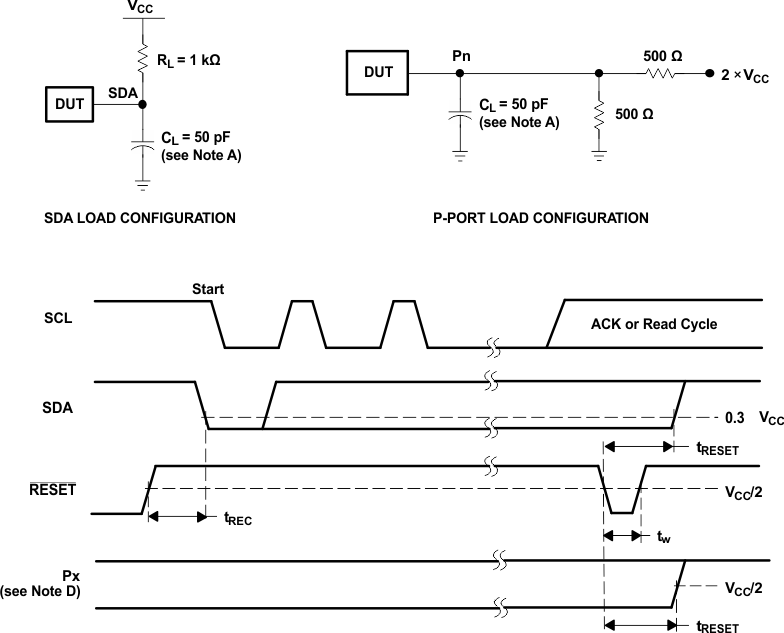
A. CL includes probe and jig capacitance.
B. All
inputs are supplied by generators having the following characteristics: PRR ≤ 10
MHz, ZO = 50 Ω, tr/tf ≤ 30 ns.
C. The
outputs are measured one at a time, with one transition per measurement.
D. I/Os are configured as inputs.
E. All
parameters and waveforms are not applicable to all devices.
Figure 7-4 Reset
Load Circuits and Voltage Waveforms