JAJSNI0 December 2021 TCAN1164-Q1
PRODUCTION DATA
- 1 特長
- 2 アプリケーション
- 3 概要
- 4 Revision History
- 5 概要 (続き)
- 6 Device Comparison Table
- 7 Pin Configurations and Functions
- 8 Specifications
- 9 Parameter Measurement Information
-
10Detailed Description
- 10.1 Overview
- 10.2 Functional Block Diagram
- 10.3
Feature Description
- 10.3.1 VSUP Pin
- 10.3.2 VCCOUT Pin
- 10.3.3 Digital Inputs and Outputs
- 10.3.4 GND
- 10.3.5 nRST Pin
- 10.3.6 SDO
- 10.3.7 nCS Pin
- 10.3.8 SCLK
- 10.3.9 SDI
- 10.3.10 CAN Bus Pins
- 10.3.11 Local Faults
- 10.3.12 Watchdog
- 10.3.13 Bus Fault Detection and Communication
- 10.4 Device Functional Modes
- 10.5
Programming
- 10.5.1 Serial Peripheral Interface (SPI) Communication
- 10.5.2 Serial Clock Input (SCLK)
- 10.5.3 Serial Data Input (SDI)
- 10.5.4 Serial Data Output (SDO)
- 10.5.5 Chip Select Not (nCS)
- 10.5.6
Registers
- 10.5.6.1 DEVICE_ID_y Register (Address = 0h + formula) [reset = xxh]
- 10.5.6.2 REV_ID_MAJOR Register (Address = 8h) [reset = 00h]
- 10.5.6.3 REV_ID_MINOR Register (Address = 9h) [reset = 00h]
- 10.5.6.4 SPI_RSVD_x Register (Address = Ah + formula) [reset = 00h]
- 10.5.6.5 Scratch_Pad_SPI Register (Address = Fh) [reset = 00h]
- 10.5.6.6 MODE_CNTRL Register (Address = 10h) [reset = 04h]
- 10.5.6.7 WD_CONFIG_1 Register (Address = 13h) [reset = 54h]
- 10.5.6.8 WD_CONFIG_2 Register (Address = 14h) [reset = 02h]
- 10.5.6.9 WD_INPUT_TRIG Register (Address = 15h) [reset = 00h]
- 10.5.6.10 WD_QA_CONFIG Register (Address = 2Dh) [reset = 0h]
- 10.5.6.11 WD_QA_ANSWER Register (Address = 2Eh) [reset = 0h]
- 10.5.6.12 WD_QA_QUESTION Register (Address = 2Fh) [reset = 0h]
- 10.5.6.13 STATUS (address = 40h) [reset = 00h]
- 10.5.6.14 INT_GLOBAL Register (Address = 50h) [reset = 0h]
- 10.5.6.15 INT_1 Register (Address = 51h) [reset = 0h]
- 10.5.6.16 INT_2 Register (Address = 52h) [reset = 40h]
- 10.5.6.17 INT_3 Register (Address 53h) [reset = 0h]
- 10.5.6.18 INT_CANBUS Register (Address = 54h) [reset = 0h]
- 10.5.6.19 INT_ENABLE_1 Register (Address = 56h) [reset = F3h]
- 10.5.6.20 INT_ENABLE_2 Register (Address = 57h) [reset = 3Fh]
- 10.5.6.21 INT_ENABLE_3 Register (Address =58h) [reset = 80h]
- 10.5.6.22 INT_ENABLE_CANBUS Register (Address = 59h) [reset = 7Fh]
- 10.5.6.23 INT_RSVD_y Register (Address = 5Ah + formula) [reset = 00h]
- 11Application Information Disclaimer
- 12Power Supply Requirements
- 13Layout
- 14Device and Documentation Support
- 15Mechanical, Packaging, and Orderable Information
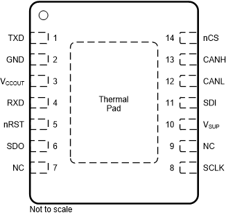
7 Pin Configurations and Functions
 Figure 7-1 DMT package, 14 Pin (VSON),
Top View
Figure 7-1 DMT package, 14 Pin (VSON),
Top ViewTable 7-1 Pin Functions
| PIN | TYPE | Description | |
|---|---|---|---|
| NAME | NO. | ||
| TXD | 1 | Digital | CAN transmit data input, integrated pull-up |
| GND | 2 | GND | Ground connection |
| VCCOUT | 3 | Supply | 5-V LDO regulated output voltage |
| RXD | 4 | Digital | CAN receive data output |
| nRST | 5 | Digital | Reset input/output |
| SDO | 6 | Digital | SPI data output |
| NC | 7 | — | No connect (not internally connected) |
| SCLK | 8 | Digital | SPI clock input |
| NC | 9 | — | No connect (not internally connected) |
| VSUP | 10 | Supply | Reverse-blocked battery supply input |
| SDI | 11 | Digital | SPI data input |
| CANL | 12 | Bus IO | Low-level CAN bus input/output line |
| CANH | 13 | Bus IO | High-level CAN bus input/output line |
| nCS | 14 | Digital | SPI chip select (active low) |