JAJSNI0 December 2021 TCAN1164-Q1
PRODUCTION DATA
- 1 特長
- 2 アプリケーション
- 3 概要
- 4 Revision History
- 5 概要 (続き)
- 6 Device Comparison Table
- 7 Pin Configurations and Functions
- 8 Specifications
- 9 Parameter Measurement Information
-
10Detailed Description
- 10.1 Overview
- 10.2 Functional Block Diagram
- 10.3
Feature Description
- 10.3.1 VSUP Pin
- 10.3.2 VCCOUT Pin
- 10.3.3 Digital Inputs and Outputs
- 10.3.4 GND
- 10.3.5 nRST Pin
- 10.3.6 SDO
- 10.3.7 nCS Pin
- 10.3.8 SCLK
- 10.3.9 SDI
- 10.3.10 CAN Bus Pins
- 10.3.11 Local Faults
- 10.3.12 Watchdog
- 10.3.13 Bus Fault Detection and Communication
- 10.4 Device Functional Modes
- 10.5
Programming
- 10.5.1 Serial Peripheral Interface (SPI) Communication
- 10.5.2 Serial Clock Input (SCLK)
- 10.5.3 Serial Data Input (SDI)
- 10.5.4 Serial Data Output (SDO)
- 10.5.5 Chip Select Not (nCS)
- 10.5.6
Registers
- 10.5.6.1 DEVICE_ID_y Register (Address = 0h + formula) [reset = xxh]
- 10.5.6.2 REV_ID_MAJOR Register (Address = 8h) [reset = 00h]
- 10.5.6.3 REV_ID_MINOR Register (Address = 9h) [reset = 00h]
- 10.5.6.4 SPI_RSVD_x Register (Address = Ah + formula) [reset = 00h]
- 10.5.6.5 Scratch_Pad_SPI Register (Address = Fh) [reset = 00h]
- 10.5.6.6 MODE_CNTRL Register (Address = 10h) [reset = 04h]
- 10.5.6.7 WD_CONFIG_1 Register (Address = 13h) [reset = 54h]
- 10.5.6.8 WD_CONFIG_2 Register (Address = 14h) [reset = 02h]
- 10.5.6.9 WD_INPUT_TRIG Register (Address = 15h) [reset = 00h]
- 10.5.6.10 WD_QA_CONFIG Register (Address = 2Dh) [reset = 0h]
- 10.5.6.11 WD_QA_ANSWER Register (Address = 2Eh) [reset = 0h]
- 10.5.6.12 WD_QA_QUESTION Register (Address = 2Fh) [reset = 0h]
- 10.5.6.13 STATUS (address = 40h) [reset = 00h]
- 10.5.6.14 INT_GLOBAL Register (Address = 50h) [reset = 0h]
- 10.5.6.15 INT_1 Register (Address = 51h) [reset = 0h]
- 10.5.6.16 INT_2 Register (Address = 52h) [reset = 40h]
- 10.5.6.17 INT_3 Register (Address 53h) [reset = 0h]
- 10.5.6.18 INT_CANBUS Register (Address = 54h) [reset = 0h]
- 10.5.6.19 INT_ENABLE_1 Register (Address = 56h) [reset = F3h]
- 10.5.6.20 INT_ENABLE_2 Register (Address = 57h) [reset = 3Fh]
- 10.5.6.21 INT_ENABLE_3 Register (Address =58h) [reset = 80h]
- 10.5.6.22 INT_ENABLE_CANBUS Register (Address = 59h) [reset = 7Fh]
- 10.5.6.23 INT_RSVD_y Register (Address = 5Ah + formula) [reset = 00h]
- 11Application Information Disclaimer
- 12Power Supply Requirements
- 13Layout
- 14Device and Documentation Support
- 15Mechanical, Packaging, and Orderable Information
10.3.12.4.1 WD Question and Answer Basic information
A Question and Answer (Q&A) watchdog is a type of watchdog where instead of simply resetting the watchdog via a SPI write or a pin toggle, the MCU reads a ‘question’ from the TCAN1164-Q1 do math based on the question and then write the computed answers back to the TCAN1164-Q1. The correct answer is a four byte response. Each byte must be written in order and with the correct timing to have a correct answer.
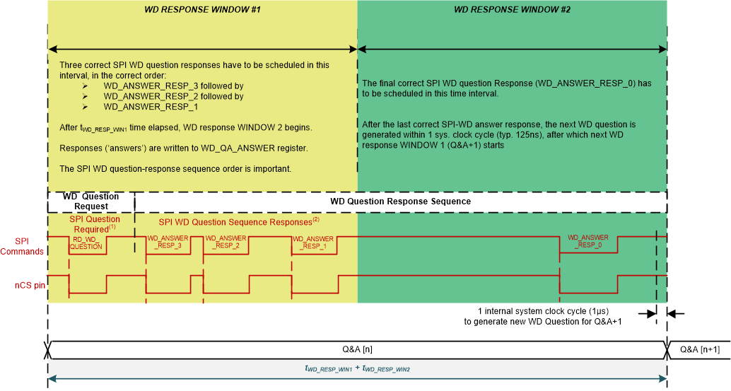
There are two watchdog windows; referred to as WD Response window #1 and WD Response window #2 (Figure 10-5 WD QA Windows as example). The size of each window will be 50% of the total watchdog time, which is selected from the WD_TIMER and WD_PRE register bits.
Each watchdog question and answer is a full watchdog cycle. The general process is the MCU reads the question, when the question is read, the timer starts. The CPU must perform a mathematical function on the question, resulting in four bytes of answers. Three of the four answer bytes must be written to the answer register within the first window, in correct order. The last answer must be written to the answer register after the first response window, inside of WD Response Window #2. If all four answer bytes were correct and in the correct order, then the response is considered good and a new question is generated, starting the cycle over again. Once the fourth answer is written into WD Response Window #2, that window is terminated and a new WD Response Window #1 is started.
If anything is incorrect or missed, the response is considered bad and the watchdog question will NOT change. In addition, an error counter will be incremented. Once this error counter hits a threshold (defined in the WD_ERR_CNT register field), the watchdog failure action will be performed. Examples of actions are an interrupt, or reset toggle, etc.
