JAJSNH9 December 2021 TCAN1167-Q1
PRODUCTION DATA
- 1 特長
- 2 アプリケーション
- 3 概要
- 4 Revision History
- 5 概要 (続き)
- 6 Pin Configurations and Functions
- 7 Specifications
- 8 Parameter Measurement Information
-
9 Detailed Description
- 9.1 Overview
- 9.2 Functional Block Diagram
- 9.3
Feature Description
- 9.3.1 VSUP Pin
- 9.3.2 VCCOUT Pin
- 9.3.3 Digital Inputs and Outputs
- 9.3.4 GND
- 9.3.5 INH Pin
- 9.3.6 WAKE Pin
- 9.3.7 nRST Pin
- 9.3.8 SDO
- 9.3.9 nCS Pin
- 9.3.10 SCLK
- 9.3.11 SDI
- 9.3.12 CAN Bus Pins
- 9.3.13 Local Faults
- 9.3.14 Watchdog
- 9.3.15 Bus Fault Detection and Communication
- 9.4 Device Functional Modes
- 9.5
Programming
- 9.5.1 Serial Peripheral Interface (SPI) Communication
- 9.5.2 Serial Clock Input (SCLK)
- 9.5.3 Serial Data Input (SDI)
- 9.5.4 Serial Data Output (SDO)
- 9.5.5 Chip Select Not (nCS)
- 9.5.6
Registers
- 9.5.6.1 DEVICE_ID_y Register (Address = 0h + formula) [reset = xxh]
- 9.5.6.2 REV_ID_MAJOR Register (Address = 8h) [reset = 00h]
- 9.5.6.3 REV_ID_MINOR Register (Address = 9h) [reset = 00h]
- 9.5.6.4 SPI_RSVD_x Register (Address = Ah + formula) [reset = 00h]
- 9.5.6.5 Scratch_Pad_SPI Register (Address = Fh) [reset = 00h]
- 9.5.6.6 MODE_CNTRL Register (Address = 10h) [reset = 04h]
- 9.5.6.7 WD_CONFIG_1 Register (Address = 13h) [reset = 54h]
- 9.5.6.8 WD_CONFIG_2 Register (Address = 14h) [reset = 02h]
- 9.5.6.9 WD_INPUT_TRIG Register (Address = 15h) [reset = 00h]
- 9.5.6.10 WD_QA_CONFIG Register (Address = 2Dh) [reset = 0h]
- 9.5.6.11 WD_QA_ANSWER Register (Address = 2Eh) [reset = 0h]
- 9.5.6.12 WD_QA_QUESTION Register (Address = 2Fh) [reset = 0h]
- 9.5.6.13 STATUS (address = 40h) [reset = 00h]
- 9.5.6.14 INT_GLOBAL Register (Address = 50h) [reset = 0h]
- 9.5.6.15 INT_1 Register (Address = 51h) [reset = 0h]
- 9.5.6.16 INT_2 Register (Address = 52h) [reset = 40h]
- 9.5.6.17 INT_3 Register (Address 53h) [reset = 0h]
- 9.5.6.18 INT_CANBUS Register (Address = 54h) [reset = 0h]
- 9.5.6.19 INT_ENABLE_1 Register (Address = 56h) [reset = F3h]
- 9.5.6.20 INT_ENABLE_2 Register (Address = 57h) [reset = 3Fh]
- 9.5.6.21 INT_ENABLE_3 Register (Address =58h) [reset = 80h]
- 9.5.6.22 INT_ENABLE_CANBUS Register (Address = 59h) [reset = 7Fh]
- 9.5.6.23 INT_RSVD_y Register (Address = 5Ah + formula) [reset = 00h]
- 10Application Information Disclaimer
- 11Power Supply Requirements
- 12Layout
- 13Device and Documentation Support
- 14Mechanical, Packaging, and Orderable Information
9.4.1.4.2 Local Wake-Up (LWU) via WAKE Input Terminal
The WAKE terminal is a bi-directional high-voltage reverse battery protected input which can be used for local wake-up (LWU) requests via a voltage transition. A LWU event is triggered on either a low-to-high or high-to-low transition since it has bi-directional input thresholds. The WAKE pin could be used with a switch to VSUP or to ground. If the terminal is unused, it should be pulled to VSUP or ground to avoid unwanted parasitic wake-up events.
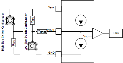
 Figure 9-16 WAKE Circuit Example
Figure 9-16 shows two possible configurations for the WAKE pin, a low-side and high-side switch configuration. The objective of the series resistor, RSERIES, is to protect the WAKE input of the device from over current conditions that may occur in the event of a ground shift or ground loss. The minimum value of RSERIES can be calculated using the maximum supply voltage, VSUPMAX, and the maximum allowable current of the WAKE pin, IIO(WAKE). RSERIES is calculated using:
If the battery voltage never exceeds 42 VDC, then the RSERIES value is approximately 10 kΩ.
The RBIAS resistor is used to set the static voltage level of the WAKE input when the switch is not in use. When the switch is in use in a high-side switch configuration, the RBIAS resistor in combination with the RSERIES resistor sets the WAKE pin voltage above the VIH threshold. The maximum value of RBIAS can be calculated using the maximum supply voltage, VSUPMAX, the maximum WAKE threshold voltage VIH, the maximum WAKE input current IIH and the series resistor value RSERIES. RBIAS is calculated using:
If the battery voltage never exceed 42 VDC, then the RBIAS resistor value must be less than 650-kΩ.
The LWU circuitry is active in sleep mode. .
The WAKE circuitry is switched off normal mode.