JAJSNH9 December 2021 TCAN1167-Q1
PRODUCTION DATA
- 1 特長
- 2 アプリケーション
- 3 概要
- 4 Revision History
- 5 概要 (続き)
- 6 Pin Configurations and Functions
- 7 Specifications
- 8 Parameter Measurement Information
-
9 Detailed Description
- 9.1 Overview
- 9.2 Functional Block Diagram
- 9.3
Feature Description
- 9.3.1 VSUP Pin
- 9.3.2 VCCOUT Pin
- 9.3.3 Digital Inputs and Outputs
- 9.3.4 GND
- 9.3.5 INH Pin
- 9.3.6 WAKE Pin
- 9.3.7 nRST Pin
- 9.3.8 SDO
- 9.3.9 nCS Pin
- 9.3.10 SCLK
- 9.3.11 SDI
- 9.3.12 CAN Bus Pins
- 9.3.13 Local Faults
- 9.3.14 Watchdog
- 9.3.15 Bus Fault Detection and Communication
- 9.4 Device Functional Modes
- 9.5
Programming
- 9.5.1 Serial Peripheral Interface (SPI) Communication
- 9.5.2 Serial Clock Input (SCLK)
- 9.5.3 Serial Data Input (SDI)
- 9.5.4 Serial Data Output (SDO)
- 9.5.5 Chip Select Not (nCS)
- 9.5.6
Registers
- 9.5.6.1 DEVICE_ID_y Register (Address = 0h + formula) [reset = xxh]
- 9.5.6.2 REV_ID_MAJOR Register (Address = 8h) [reset = 00h]
- 9.5.6.3 REV_ID_MINOR Register (Address = 9h) [reset = 00h]
- 9.5.6.4 SPI_RSVD_x Register (Address = Ah + formula) [reset = 00h]
- 9.5.6.5 Scratch_Pad_SPI Register (Address = Fh) [reset = 00h]
- 9.5.6.6 MODE_CNTRL Register (Address = 10h) [reset = 04h]
- 9.5.6.7 WD_CONFIG_1 Register (Address = 13h) [reset = 54h]
- 9.5.6.8 WD_CONFIG_2 Register (Address = 14h) [reset = 02h]
- 9.5.6.9 WD_INPUT_TRIG Register (Address = 15h) [reset = 00h]
- 9.5.6.10 WD_QA_CONFIG Register (Address = 2Dh) [reset = 0h]
- 9.5.6.11 WD_QA_ANSWER Register (Address = 2Eh) [reset = 0h]
- 9.5.6.12 WD_QA_QUESTION Register (Address = 2Fh) [reset = 0h]
- 9.5.6.13 STATUS (address = 40h) [reset = 00h]
- 9.5.6.14 INT_GLOBAL Register (Address = 50h) [reset = 0h]
- 9.5.6.15 INT_1 Register (Address = 51h) [reset = 0h]
- 9.5.6.16 INT_2 Register (Address = 52h) [reset = 40h]
- 9.5.6.17 INT_3 Register (Address 53h) [reset = 0h]
- 9.5.6.18 INT_CANBUS Register (Address = 54h) [reset = 0h]
- 9.5.6.19 INT_ENABLE_1 Register (Address = 56h) [reset = F3h]
- 9.5.6.20 INT_ENABLE_2 Register (Address = 57h) [reset = 3Fh]
- 9.5.6.21 INT_ENABLE_3 Register (Address =58h) [reset = 80h]
- 9.5.6.22 INT_ENABLE_CANBUS Register (Address = 59h) [reset = 7Fh]
- 9.5.6.23 INT_RSVD_y Register (Address = 5Ah + formula) [reset = 00h]
- 10Application Information Disclaimer
- 11Power Supply Requirements
- 12Layout
- 13Device and Documentation Support
- 14Mechanical, Packaging, and Orderable Information
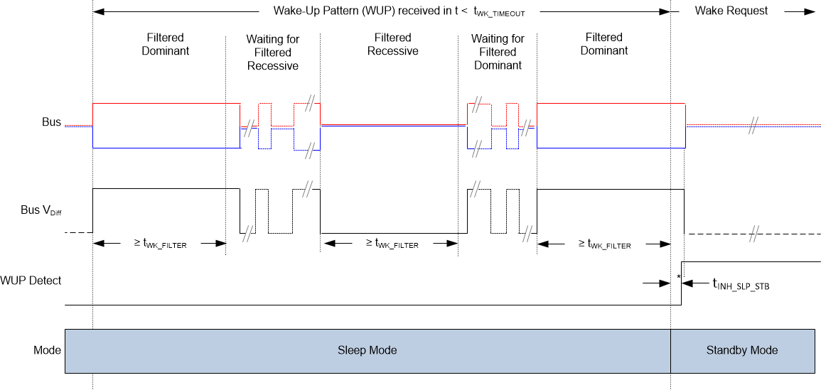
9.4.1.4.1 Remote Wake Request via Wake-Up Pattern (WUP)
The TCAN1167-Q1 implements a low-power wake receiver in the standby and sleep mode that uses the multiple filtered dominant wake-up pattern (WUP) defined in the ISO11898-2:2016 standard.
The wake-up pattern (WUP) consists of a filtered dominant bus, then a filtered recessive bus time followed by a second filtered bus time. The first filtered dominant initiates the WUP and the bus monitor is now waiting on a filtered recessive, other bus traffic do not reset the bus monitor. Once a filtered recessive is received, the bus monitor is now waiting on a filtered dominant. The other bus traffic do not reset the bus monitor. Immediately upon receiving of the second filtered dominant, the bus monitor recognizes the WUP and drives the RXD terminal low.
The WUP consists of:
- A filtered dominant bus of at least tWK_FILTER followed by
- A filtered recessive bus time of at least tWK_FILTER followed by
- A second filtered dominant bus time of at least tWK_FILTER
For a dominant or recessive to be considered “filtered”, the bus must be in that state for more than tWK_FILTER time. Due to variability in the tWK_FILTER the following scenarios are applicable. Bus state times less than tWK_FILTER(MIN) are never detected as part of a WUP, and thus no wake request is generated. Bus state times between tWK_FILTER(MIN) and tWK_FILTER(MAX) may be detected as part of a WUP, and a wake request may be generated. Bus state times more than tWK_FILTER(MAX) are always detected as part of a WUP, and thus a wake request is generated. See Figure 9-15 for the timing diagram of the WUP.
The pattern and tWK_FILTER time used for the WUP and wake request prevents noise and bus stuck dominant faults from causing false wake requests while allowing any CAN or CAN FD message to initiate a wake request.
ISO11898-2:2016 has two sets of times for a short and long wake-up filter times. The tWK_FILTER timing for the TCAN1167-Q1 has been picked to be within the min and max values of both filter ranges. This timing has been chosen such that a single bit time at 500 kbps, or two back to back bit times at 1 Mbps triggers the filter in either bus state.
For an additional layer of robustness and to prevent false wake-ups, the device implements the tWK_TIMEOUT timer. For a remote wake-up event to successfully occur, the entire wake-up pattern must be received within the timeout value. If a the full wake-up pattern is notreceived before the tWK_TIMEOUT expires, then the internal logic is reset and the device remains in sleep mode without waking up. The full pattern must then be transmitted again within the tWK_TIMEOUT window. See Figure 9-15.
 Figure 9-15 Wake-Up Pattern (WUP) From Sleep Mode To Standby Mode