JAJSV18 July 2024 TCAN1473A-Q1
ADVANCE INFORMATION
- 1
- 1 特長
- 2 アプリケーション
- 3 概要
- 4 Pin Configuration and Functions
-
5 Specifications
- 5.1 Absolute Maximum Ratings
- 5.2 ESD Ratings
- 5.3 ESD Ratings - IEC Specifications
- 5.4 Recommended Operating Conditions
- 5.5 Thermal Information
- 5.6 Power Dissipation Ratings
- 5.7 Power Supply Characteristics
- 5.8 Electrical Characteristics
- 5.9 Timing Requirements
- 5.10 Switching Characteristics
- 5.11 Typical Characteristics
- 6 Parameter Measurement Information
-
7 Detailed Description
- 7.1 Overview
- 7.2 Functional Block Diagram
- 7.3
Feature Description
- 7.3.1 Supply Pins
- 7.3.2 Digital Inputs and Outputs
- 7.3.3 GND
- 7.3.4 INH Pin
- 7.3.5 WAKE Pin
- 7.3.6 CAN Bus Pins
- 7.3.7
Faults
- 7.3.7.1
Internal and External Fault Indicators
- 7.3.7.1.1 Power-Up (PWRON Flag)
- 7.3.7.1.2 Wake-Up Request (WAKERQ Flag)
- 7.3.7.1.3 Undervoltage Faults
- 7.3.7.1.4 CAN Bus Fault (CBF Flag)
- 7.3.7.1.5 TXD Clamped Low (TXDCLP Flag)
- 7.3.7.1.6 TXD Dominant State Timeout (TXDDTO Flag)
- 7.3.7.1.7 TXD Shorted to RXD Fault (TXDRXD Flag)
- 7.3.7.1.8 CAN Bus Dominant Fault (CANDOM Flag)
- 7.3.7.1
Internal and External Fault Indicators
- 7.3.8 Local Faults
- 7.4 Device Functional Modes
- 8 Application Information Disclaimer
- 9 Device and Documentation Support
- 10Revision History
- 11Mechanical, Packaging, and Orderable Information
パッケージ・オプション
デバイスごとのパッケージ図は、PDF版データシートをご参照ください。
メカニカル・データ(パッケージ|ピン)
- D|14
- DYY|14
- DMT|14
サーマルパッド・メカニカル・データ
発注情報
6 Parameter Measurement Information
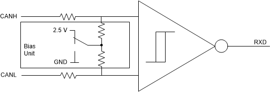
 Figure 6-1 Common-Mode Bias Unit and Receiver
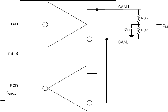
 Figure 6-2 Test Circuit
 Figure 6-3 Supply Test Circuit
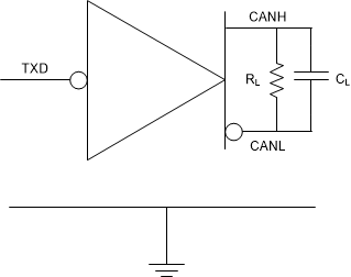
 Figure 6-4 Driver Test Circuit and Measurement
 Figure 6-5 Receiver Test Circuit and Measurement
 Figure 6-6 Transmitter and Receiver Timing Behavior Test Circuit and Measurement
 Figure 6-7 TXD Dominant Time Out Test Circuit and Measurement
 Figure 6-8 Driver Short-Circuit Current Test and Measurement
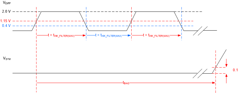
 Figure 6-9 Bias Reaction Time Measurement
- nFAULT clears upon exiting silent mode

- nFAULT clears upon exiting silent mode
 Figure 6-12 Power-Up Timing
 Figure 6-13 SIC Timing and impedance
during the active and passive recessive phase.